

Particle-optical inspection device especially for semiconductor wafers
a technology of optical inspection and semiconductor wafers, applied in semiconductor/solid-state device testing/measurement, material analysis using wave/particle radiation, instruments, etc., can solve the problems of inability to compare real-time patterns, device complexity is much more complex than in the case of fixed relative, and achieves the effect of preventing magnetic saturation
- Summary
- Abstract
- Description
- Claims
- Application Information
AI Technical Summary
Benefits of technology
Problems solved by technology
Method used
Image

Examples
Embodiment Construction
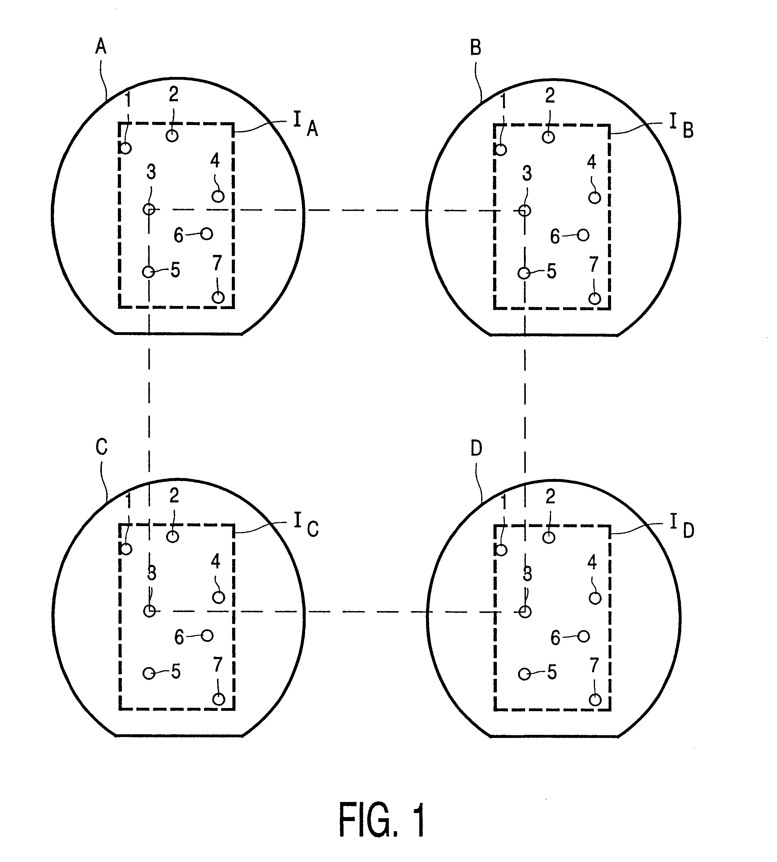
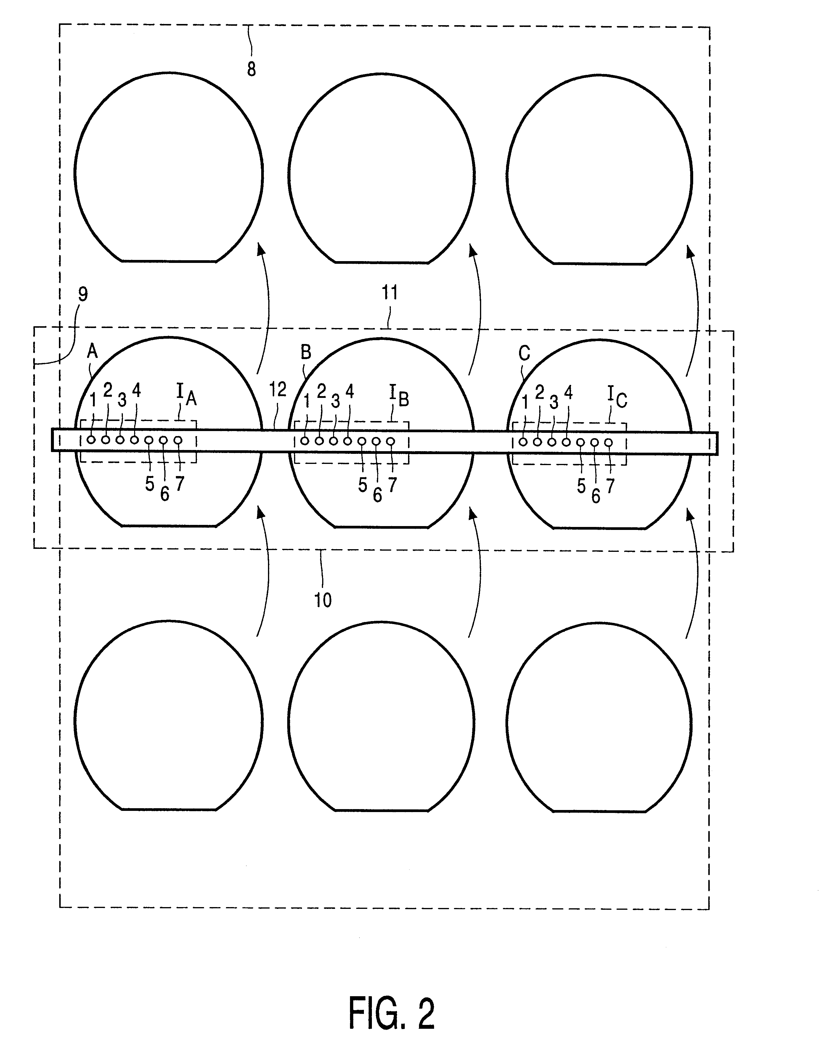
In order to illustrate the idea of the invention FIG. 1 shows a number of wafers A to D and an inspection unit I.sub.A -I.sub.D for each wafer, each of said inspection units I being provided with seven particle-optical columns 1 to 7 for scanning the pattern to be inspected on the associated wafer. The particle-optical columns are constructed as electron optical columns. The electron optical columns 1 to 7 are arranged in the same way in each inspection unit and the inspection units I.sub.A -I.sub.D are also arranged in the same way relative to the wafers A to D; this means that, for example, the column 1 in the inspection unit I.sub.A occupies the same position relative to the wafer A as the column 1 in the inspection unit IB relative to the wafer B.
The electron optical columns 1 to 7 may occupy a fixed position relative to the wafers A to D during the execution of an inspection scan, the wafers then being stationary relative to the complete inspection apparatus in which the inspec...
PUM
 Abstract
Description
Claims
Application Information