
Enhanced electrical/mechanical connection for electronic devices

a technology of electrical/mechanical connection and electronic device, which is applied in the direction of fixed connection, coupling device connection, printed circuit manufacturing, etc., can solve the problems of assembly being subject to heating and cooling cycles, adhesive or solder may "wick" through the connector array, and in undesirable fashion,

Inactive Publication Date: 2004-02-24
GOOGLE LLC
View PDF23 Cites 54 Cited by
  • Summary
  • Abstract
  • Description
  • Claims
  • Application Information

AI Technical Summary

Benefits of technology

The present invention relates to a structure and method for mechanically and electrically connecting electronic modules to printed circuit boards through a plurality of compliant electrical conductors attached to contact surfaces on both the module and the PCB. The invention aims to improve the fatigue life of the connection by addressing the challenges of aligning the contacts, providing a reliable connection with a satisfactory performance relating to stable contact resistance and fatigue life, and preventing the permanent adhesive or solder from spreading beyond the desired attachment interface. The invention also addresses the issue of shear strain caused by heating and cooling cycles and vibration forces, and provides a solution for achieving a secure and reliable connection between the module and PCB contacts.

Problems solved by technology

And, lastly, where the conductive connector is permanently attached to one or both of the module and PCB contacts with solder or some other permanent adhesive compound, the adhesive or solder may "wick" through the connector array and spread in an undesirable fashion, perhaps even creating electrical "shorts" between adjacent connectors or contacts.
During the operation of this assembly in a typical computing application, the assembly will be subject to heating and cooling cycles inherent in the electrical and mechanical use of the assembly.
Since they will expand and contract at different rates, the ceramic module and epoxy resin PCB will necessarily move with respect to each other during heating and cooling cycles, resulting in shear forces acting upon module and PCB contact connections.
However, solder column technologies are more difficult to form due to cast in place or clasp and attach processes.
Furthermore, since solder connections deform inelastically and in response to thermal mismatch shear displacements, multiple heating and cooling cycles can eventually cause solder connections to fail.
Moreover, as the array density of the connectors increases, the application of solder to the contacts is problematic in preventing the solder from spreading outside of the contact areas and causing undesirable shorts between adjacent contacts.
Nickel, tin, copper and aluminum surfaces provide much higher contact resistance that has significant resistance drift during stress and are, therefore, less suitable for demanding microelectronics interconnection.

Method used


Image

  • Enhanced electrical/mechanical connection for electronic devices
  • Enhanced electrical/mechanical connection for electronic devices
  • Enhanced electrical/mechanical connection for electronic devices

Examples


Embodiment Construction

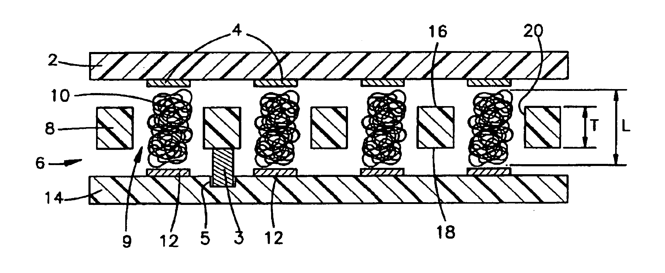
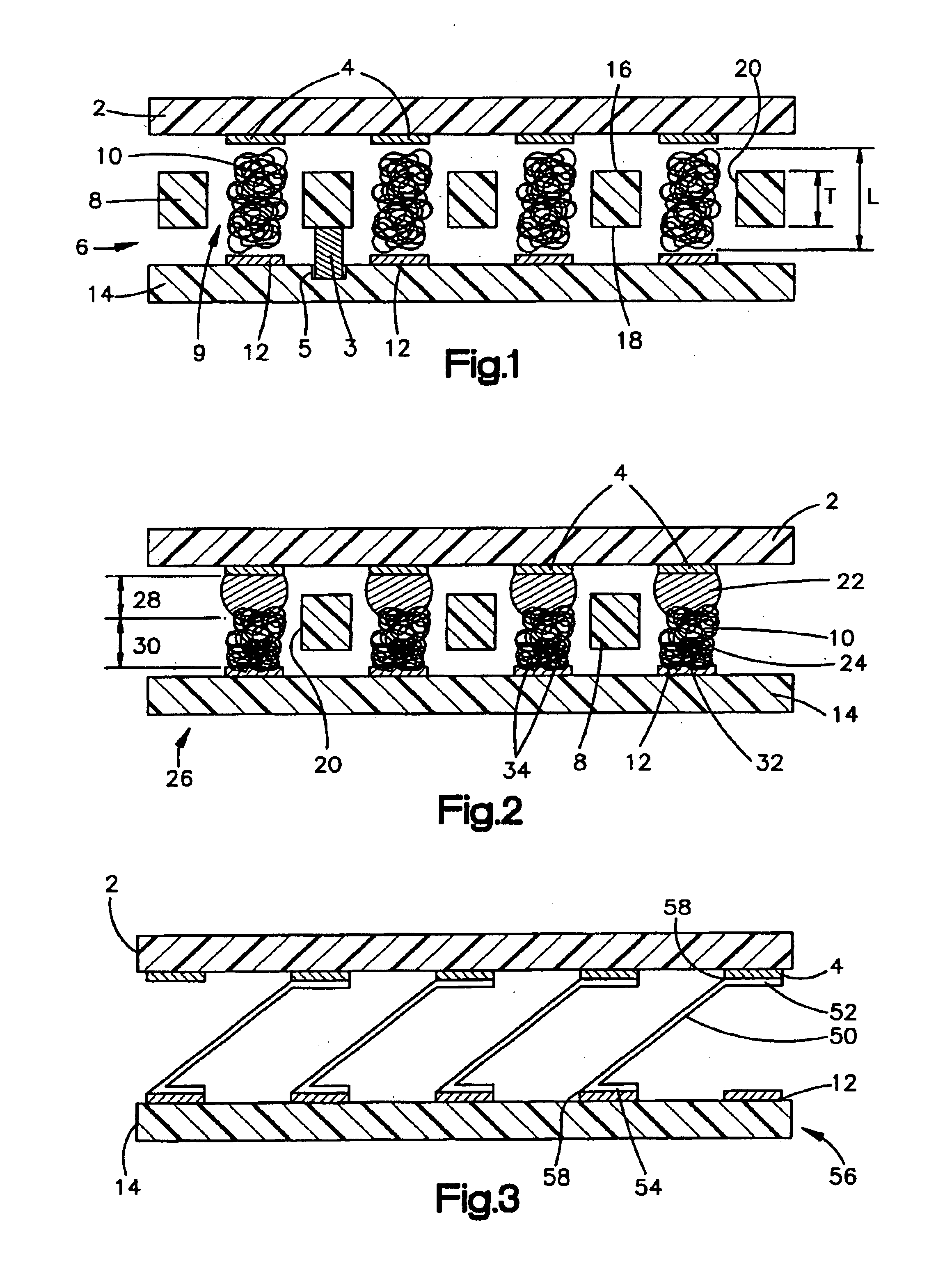
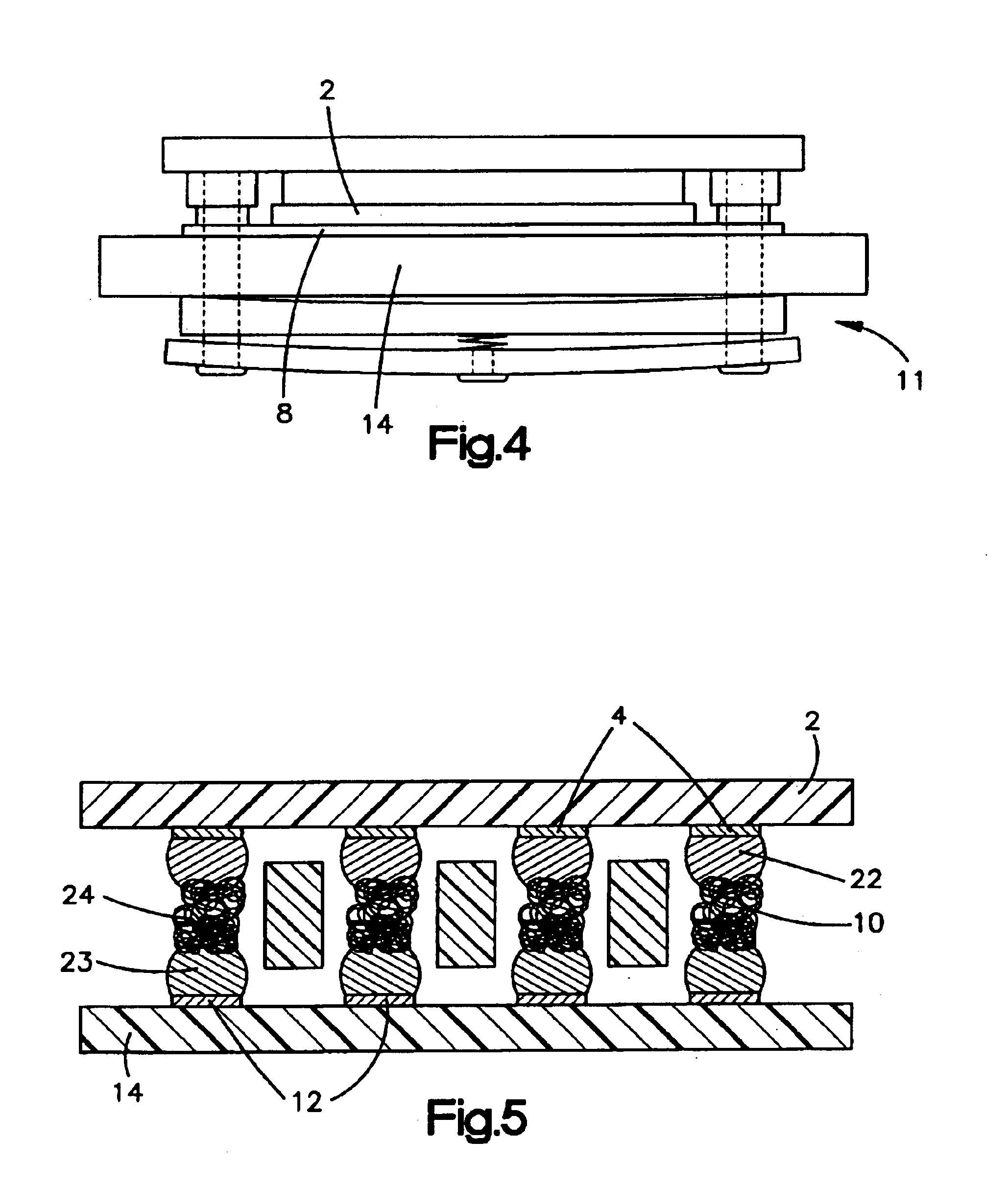
(not shown), an electrically conductive adhesive, specifically Ablebond 8175 made by Ablestick Laboratories, is applied to the PCB contacts 12. The adhesive is applied by a stencil deposit method, using a 0.005" thick stencil with an array of 0.020" diameter apertures corresponding to the PCB contact 12 array. The adhesive deposits are 0.020" in diameter, are hemispherically shaped and are between 0.003-0.004" tall. After aligning mechanical alignment pins 3 located on the interposer S with receiving holes 5 formed on the PCB 14, the conductors 10 are brought into contact with the electrically conductive adhesive deposit After adhesive cure, four point probe measurements of the interconnection between PCB 14 backside and interposer 8 backside showed a low contact resistance in the range of about 5 to about 40 milliohms. (There is some variable probe contact resistance in these measurements that may be as high as about 20 to about 30 milliohms). The PCB contacts 12 were gold plated a...


PUM

PropertyMeasurementUnit
diameteraaaaaaaaaa
diameteraaaaaaaaaa
diameteraaaaaaaaaa

Abstract

A method and structure for electrically and mechanically interconnecting an array of printed circuit board contacts to an array of module contacts with a plurality of deformable resilient electrical conductors with two ends. Each of the conductor ends are electrically connected to one of the contact arrays. A portion of the conductor may deform longitudinally and laterally responsive to movement of the printed circuit board relative to the module responsive to heating and cooling cycles and mechanical vibrations, while maintaining the electrical connection of the contact arrays. An interposer with apertures extending through the interposer carries the conductors in the apertures and is used to align the conductors with the contacts. A method for excluding a rigid adhesive means from a portion of the resilient conductor is also taught.

Description

The present invention relates to the mounting of electronic modules upon printed circuit boards and, more particularly, to a structure and method for mechanically and electrically connecting the module to the printed circuit board through a plurality of compliant electrical conductors attached to contact surfaces, said connection having an improved fatigue life.BACKGROUND OF INVENTIONIn many computer and other electronic circuit structures, an electronic module such as a Central Processor Unit (CPU), memory module or ASIC, must be connected to a printed circuit board (hereinafter sometimes "PCB"). In connecting a module to a PCB, a plurality of individual electrical contacts on the base of the module must be connected to a plurality of corresponding individual electrical contacts on the PCB. This set of contacts on the PCB dedicated to receiving the module contacts is known as a land grid array (hereinafter sometimes "LGA") site.The required interconnect density on today's printed c...

Claims


Application Information

Patent Timeline
Patent Type & Authority Patents(United States)
IPC IPC(8): H05K3/32H05K3/34
CPCH05K3/325H01R12/52H05K3/321Y10T29/49147Y10T29/49149H05K3/3436
Inventor BRODSKY, WILLIAM LOUISCALETKA, DAVID V.GAYNES, MICHAEL ANTHONYMARKOVICH, VOYA RISTA
Owner GOOGLE LLC
Learn More