Digital switching amplifier

a digital switching amplifier and amplifier technology, applied in the field of digital switching amplifiers, can solve the problems of offset voltage, noise in the lower frequency band, and inability to obtain a target frequency band and a target dynamic rang

Inactive Publication Date: 2004-03-02
SHARP KK
View PDF7 Cites 17 Cited by
  • Summary
  • Abstract
  • Description
  • Claims
  • Application Information

AI Technical Summary

Benefits of technology

As described above, even when the attenuation factors are different between the attenuation sections, the D.C. voltage level difference of the negative feedback signals that are returned to the delta sigma modulation circuit becomes substantially zero (the absolute D.C. voltage levels of the differential negative feedback signals are coincident with each other). This allows to ensurely avoid that the gain of the digital switching amplifier changes and to easily avoid that the noise occurs in the lower frequency band due to the offset voltage, because the transfer characteristics, that the algorithm requires, are maintained in the digital sigma modulation circuit. Further, it is possible to prevent from occurring that (a) the remaining noise increases or (b) the maximum permissible doses (oscillation limits) of the differential input signals with regard to the negative feedback signals respectively change. Namely, it is prevented from occurring that the maximum output of the digital switching amplifier changes and the S / N ratio becomes lowered. This allows to ensurely obtain a target frequency band and a target dynamic range.
With the arrangement, the output signals of the respective attenuation sections are sent to the delta sigma modulation circuit via the first and second resistors. Meanwhile, the predetermined analog voltage or the ground level is applied to the rheostat via the movable terminal. This allows the resistances on both sides of the movable terminal in the rheostat to vary depending on the movement of the movable terminal of the rheostat. The adjustment voltages vary depending on the respective resistances. The adjustment voltages are added to the output signals of the respective attenuation sections and are adjusted so that the D.C. voltage level difference between the negative feedback signals which return to the delta sigma modulation circuit becomes substantially zero. Since it is possible to make the absolute D.C. voltage levels of the differential negative feedback signals be equal to each other, it is possible (a) to ensurely avoid that the gain of the digital switching amplifier changes and (b) to easily avoid that the noise occurs in the lower frequency band due to the offset voltage.
As described above, even when the attenuation factors are different between the attenuation sections, the D.C. voltage level difference of the negative feedback signals that are returned to the delta sigma modulation circuit becomes substantially zero (the absolute D.C. voltage levels of the differential negative feedback signals are coincident with each other). This allows to ensurely avoid that the gain of the digital switching amplifier changes and to easily avoid that the noise occurs in the lower frequency band due to the offset voltage, because the transfer characteristics, that the algorithm requires, are maintained in the digital sigma modulation circuit. Further, it is possible to prevent from occurring that (a) the remaining noise increases or (b) the maximum permissible doses (oscillation limits) of the differential input signals with regard to the negative feedback signals respectively change. Namely, it is prevented from occurring that the maximum output of the digital switching amplifier changes and the S / N ratio becomes lowered. This function allows a target frequency band and a target dynamic range to be obtained.
With the arrangement, the 1-bit signals that have been subjected to the power amplification are sent to the delta sigma modulation circuit via the first and second resistors. Meanwhile, the predetermined analog voltage or the ground level is applied to the rheostat via the movable terminal. This allows the resistances on both sides of the movable terminal in the rheostat to vary depending on the movement of the movable terminal of the rheostat. The adjustment voltages vary depending on the respective resistances. The adjustment voltages are added to the 1-bit signals that have been subjected to the power amplification and are adjusted so that the D.C. voltage level difference between the negative feedback signals which return to the delta sigma modulation circuit becomes substantially zero. Since it is possible to make the absolute D.C. voltage levels of the differential negative feedback signals be equal to each other, it is possible (a) to ensurely avoid that the gain of the digital switching amplifier changes and (b) to easily avoid that the noise occurs in the lower frequency band due to the offset voltage.

Problems solved by technology

This causes the occurrence of a noise in the lower frequency band.
This causes such an offset voltage.
However, according to the foregoing offset voltage adjustment, since the D.C. voltage levels of the negative feedback signals S4P and S4M are respectively adjusted by changing the attenuation factors of the respective variable attenuators 9P and 9M, the following problem arises.
This causes the problem that it is not possible to obtain a target frequency band and a target dynamic range.
This causes the occurrence of a noise in the lower frequency band.
However, the adjustment of the attenuation factors of the respective attenuation sections causes the following new problem.
When adopting two channels of the conventional digital switching amplifiers that are connected in parallel with each other as a stereo amplifier for amplifying a stereo acoustic signal, it is most likely that there occurs a volume difference between the light and left channels.
Further, since the transfer characteristics, that the algorithm requires, are not maintained when integration and addition are made by the delta sigma modulation circuit so as to be noise-shaped, (a) the remaining noise increases or (b) the maximum permissible doses (oscillation limits) of the differential input signals with regard to the negative feedback signals respectively change.
This causes the problem that it is not possible to obtain a target frequency band and a target dynamic range.

Method used


Image

  • Digital switching amplifier
  • Digital switching amplifier
  • Digital switching amplifier

Examples


Embodiment Construction

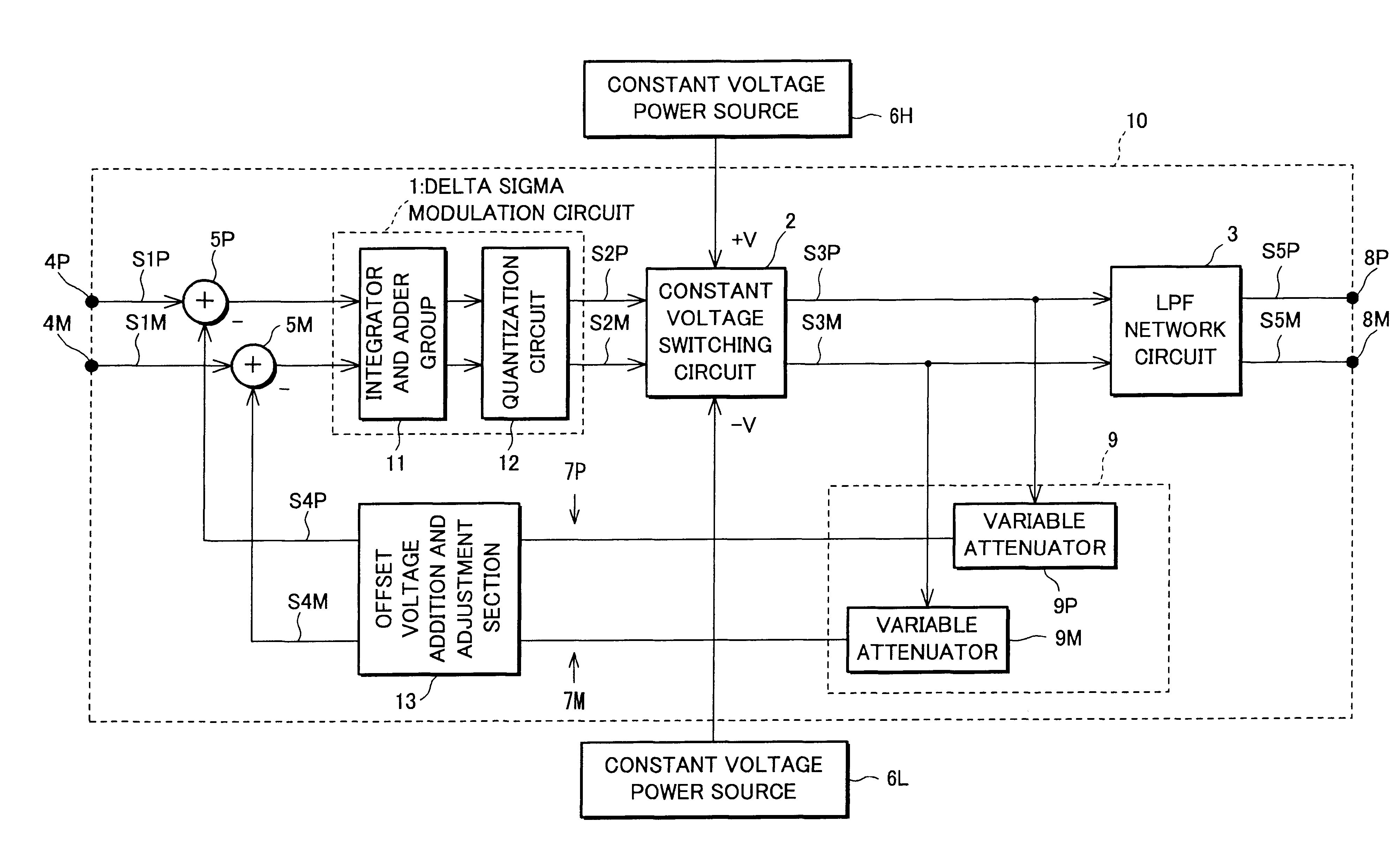
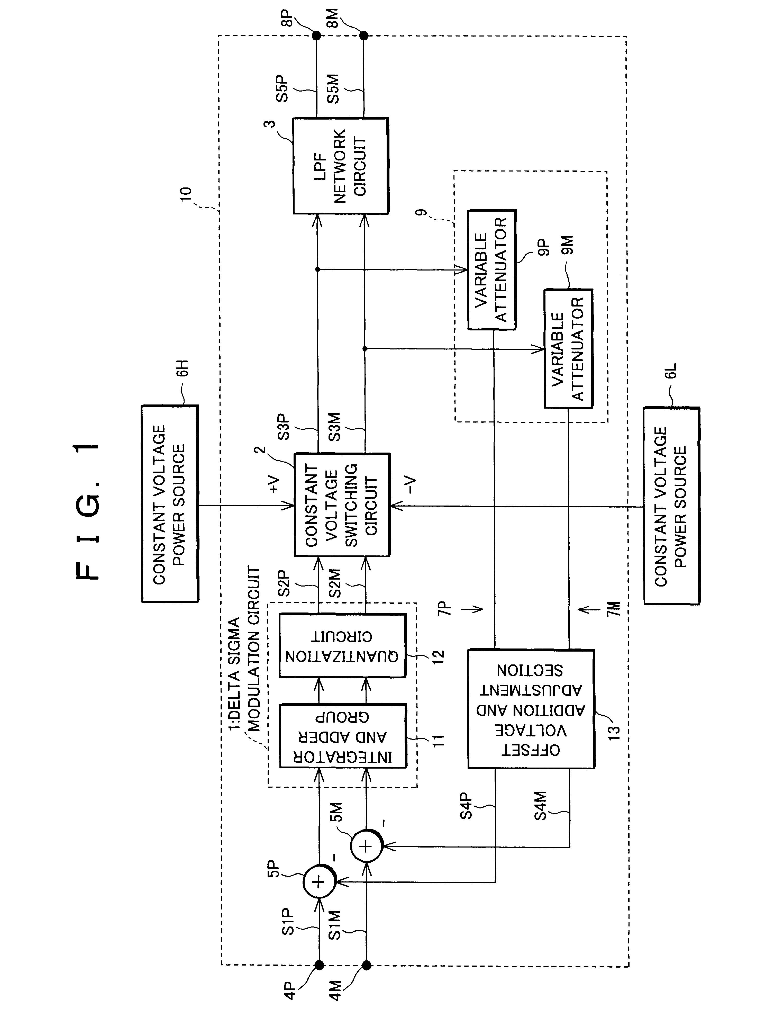
The following description deals with one embodiment of the present invention with reference to FIGS. 1 through 4. Note that the same reference numerals are assigned to the members that have the same functions as those shown in FIG. 5.

As shown in FIG. 1, differential input signals are inputted via input terminals 4P and 4M to a digital switching amplifier 10 according to the present invention. The differential input signal is made of a pair of an analog acoustic signal S1P having a positive polarity and an analog acoustic signal S1M having a negative polarity. A delta sigma modulation circuit 1 converts the analog acoustic signals S1P and S1M into 1-bit signals S2P and S2M, respectively. Then, the 1-bit signals S2P and S2N are sent to a constant voltage switching circuit 2 in which constant voltages (+V and -V) are switched and amplified in accordance with the 1-bit signals S2P and S2M so as to be demodulated to analog acoustic signals S52 and S5M by a low pass filter network circuit...


PUM


Abstract

A digital switching amplifier is provided with attenuation sections that attenuate respective 1-bit signals that have been subjected to the power amplification. Also, an offset voltage addition and adjustment section adds adjustment voltages to output signals of the respective attenuation sections so that a D.C. voltage level difference between negative feedback signals which return to a delta sigma modulation circuit becomes substantially zero. This function ensures that the digital switching amplifier can avoid the gain with respect to positive and negative input signals change and easily avoid the noise that occurs in the lower frequency band due to an offset voltage.

Description

FIELD OF THE INVENTIONThe present invention relates to a digital switching amplifier capable of amplifying 1-bit conversion signal, with high efficiency, that is obtained by converting an analog signal or a multi-bit signal in accordance with the delta sigma modulation.DESCRIPTION OF RELATED ARTA 1-bit signal is obtained by the delta sigma modulation is not limited to be used for recording an audio signal and transmitting among the electronic devices. It is also possible to obtain a demodulated analog signal that has been subjected to the power amplification, only by (a) sending the 1-bit signal, as it is, to a semiconductor power amplifier device so as to obtain switching pulses having a great amplitude of voltage and (b) filtering the switching pulses through a low pass filter.Further, in the semiconductor power amplifier device a nonlinear region (a saturated region) is used for its operations, unlike the conventional amplifier in which a linear region (an unsaturated region) is ...

Claims


Application Information

Patent Timeline
Patent Type & Authority Patents(United States)
IPC IPC(8): H03F3/217H03F3/20H03M3/02H03F3/34
CPCH03F3/217H03M3/356H03F2200/331H03M3/43H03M3/438
Inventor KISHIDA, MASAHIRO
Owner SHARP KK
Why Eureka
Try Eureka