Exposure method and exposure apparatus

a technology of exposure apparatus and exposure method, which is applied in the direction of photomechanical apparatus, instruments, printing, etc., can solve the problems of inapplicability of mechanical switching the shape of the opening inability to meet the integral number of pulses, and inability to apply mechanical switching the shape of the field diaphragm

Inactive Publication Date: 2004-03-09
MITUTOYO CORP +1
View PDF36 Cites 22 Cited by
  • Summary
  • Abstract
  • Description
  • Claims
  • Application Information

AI Technical Summary

Benefits of technology

A second object of the present invention is to provide an exposure method which makes it possible to enhance the uniformity of a totalized exposure amount on a wafer when the scanning exposure is performed by using a pulse light beam as an exposure light beam.
A method for producing a device according to the present invention comprises the step of transferring a device pattern (R) onto a workpiece (W) by using the exposure method of the present invention. The uniformity of the totalized exposure amount is improved by the present invention. Therefore, it is possible to highly accurately mass-produce devices having high degrees of integration.

Problems solved by technology

In this case, if the shape of the opening of the field diaphragm is mechanically switched, it is feared that any area appears on the wafer, in which the condition of exposure in the amount corresponding to the integral number of pulses is not satisfied.
Therefore, the method for mechanically switching the shape of the opening of the field diaphragm is not practical so much.
As a result, the transmittance of the optical system is lowered over a long period of time.
As a result, it is feared that the distribution of illuminance is not uniform in the non-scanning direction in the illumination area (or the exposure area), and the unevenness of the totalized exposure amount is increased.
Further, if the variation of the transmittance occurs about the center of any point other than those disposed on the optical axis, it is also feared that the collapse amount of the telecentricity (telecentric property) of the exposure light beam with respect to the reticle or the wafer exceeds an allowable range.
However, it takes a fairly long period of time to perform the exchange.
However, in such a case, the exposure apparatus has a large size, and the production cost is increased as well.

Method used


Image

  • Exposure method and exposure apparatus
  • Exposure method and exposure apparatus
  • Exposure method and exposure apparatus

Examples


first modified embodiment

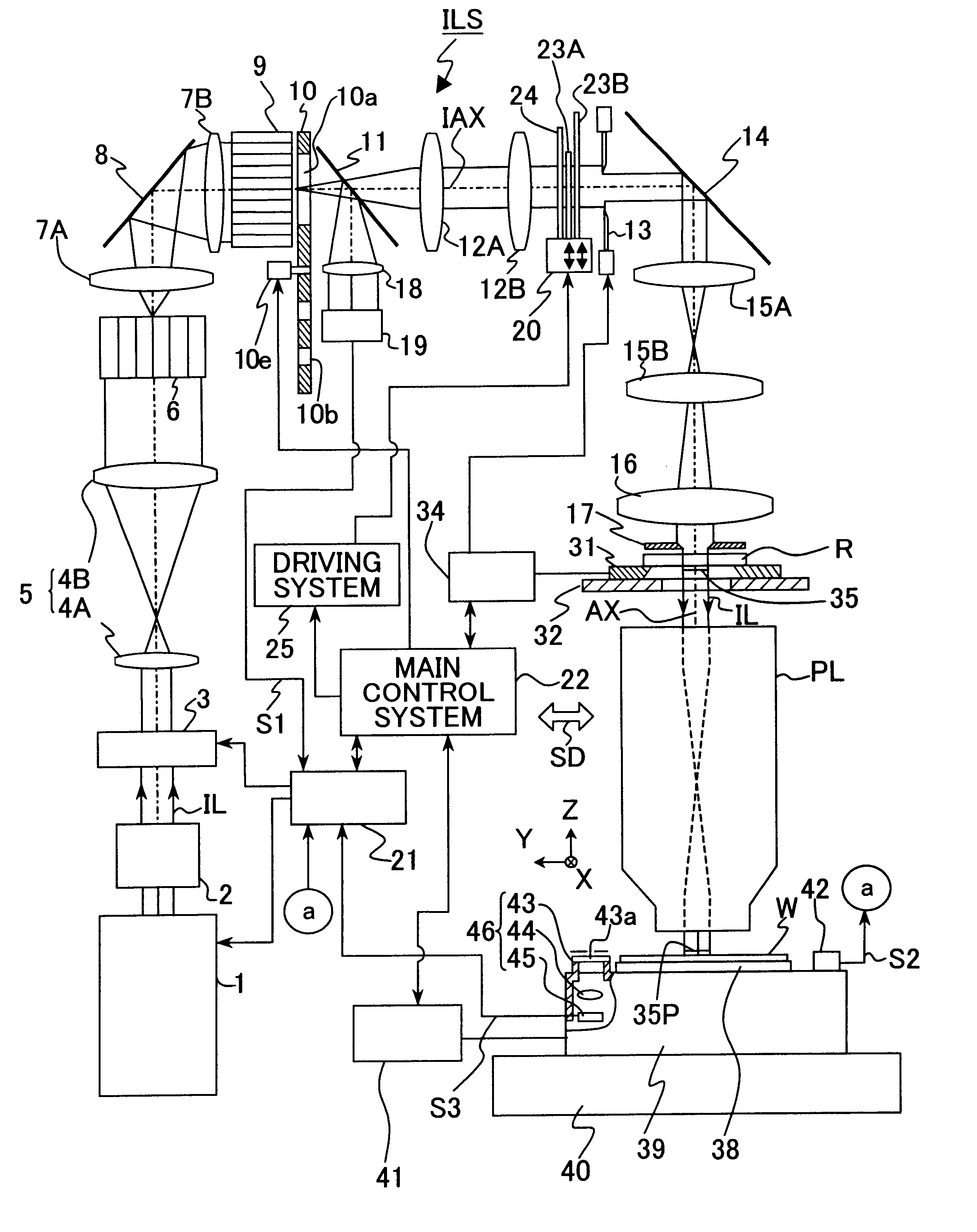
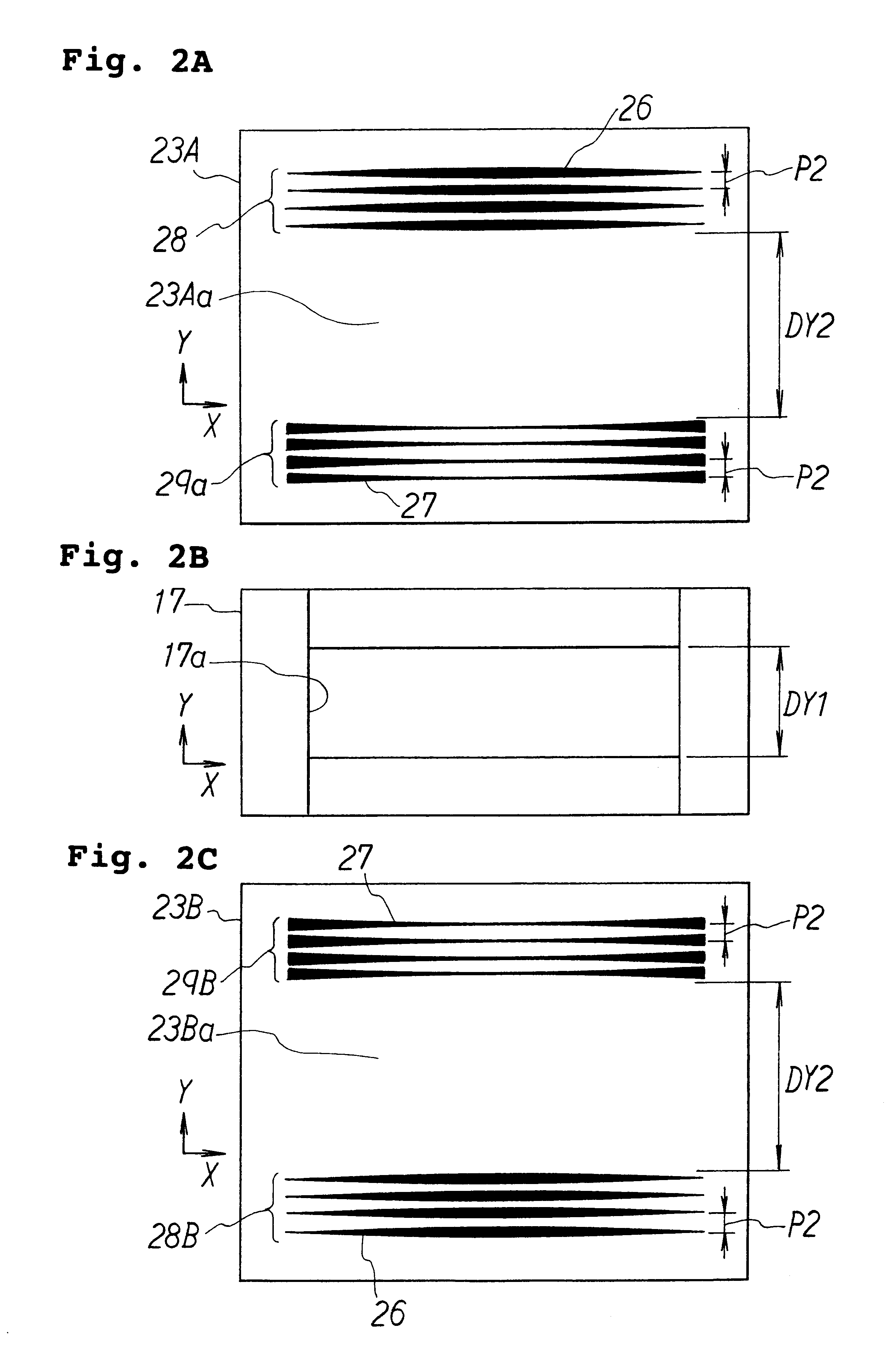
FIG. 10 shows uneven illuminance-correcting plates 23C, 23D of a first modified embodiment as illustrated corresponding to the uneven illuminance-correcting plates 23A, 23B shown in FIG. 8A. With reference to FIG. 10, two pairs of convex uneven illuminance-correcting shielding line groups 28A and two pairs of concave uneven illuminance-correcting shielding line groups 29A are formed in parallel on the first uneven illuminance-correcting plate 23C. Two pairs of shielding line groups 28B and two pairs of shielding line groups 29B are formed in parallel on the second uneven illuminance-correcting plate 23D. That is, the shielding line groups are formed on each of the uneven illuminance-correcting plates 23C, 23D in an area which is twice as large as that of each of the uneven illuminance-correcting plates 23A, 23B shown in FIG. 8. In this arrangement, the entire area of the image of the opening 17a of the fixed blind 17 (illumination area 35) can be covered with the shielding line grou...

second modified embodiment

FIG. 11A shows an uneven illuminance-correcting plate of a With reference to FIG. 11A, shielding lines 64A, 64B for correcting the concave uneven illuminance, in which the line width is gradually changed in the non-scanning direction (X direction), are depicted on unillustrated two transmissive substrates. The shielding lines 64A, 64B (unillustrated substrates) are constructed so that they may be continuously driven independently in the X direction with respect to the illumination area 35 on the reticle. In this modified embodiment, in order to correct the concave uneven illuminance in the non-scanning direction, the shielding lines 64A, 64B are gradually moved inwardly in the X direction as shown in FIGS. 11B and 11C depending on the increase in degree of the uneven illuminance. When the two shielding lines 64A, 64B are arranged centrally asymmetrically with respect to the illumination area 35 as described above, the telecentric discrepancy can be also corrected continuously toget...

third modified embodiment

FIG. 12 shows a shielding line of a FIG. 12A illustrates the shielding line 26 used in the embodiment shown in FIG. 8. FIG. 12B illustrates a shielding pattern 66 in which identical dot patterns composed of a large number of minute shielding films are depicted with a density distribution to make change, for example, substantially in a form of quadratic function with respect to the non-scanning direction so as to possess substantially the same shielding characteristic as that of the shielding line 26. The shielding pattern 66 can be used in place of the shielding line 26. Accordingly, it is possible to further reduce the uneven illuminance during the static exposure.

As for the shielding pattern 66, the spacing distances between the respective adjoining dot patterns are set as randomly as possible so that no uneven illuminance is caused by the occurrence of any speckle pattern in the illumination area on the reticle. In place of the control of the density distribution of the large nu...


PUM

PropertyMeasurementUnit
wavelengthaaaaaaaaaa

Abstract

An exposure apparatus transfers an image of a pattern on a reticle onto a wafer W by synchronously scanning the reticle and the wafer with respect to a projection optical system in a state in which the reticle is illuminated with an exposure light beam from an exposure light source subjected to pulse light emission via a fly's eye lens, a movable blind, a main condenser lens system, and a fixed blind. First and second uneven illuminance-correcting plates, on which shielding line groups for correcting convex and concave uneven illuminance are depicted, are arranged at a position defocused from a conjugate plane with respect to a pattern plane of the reticle. A third correcting plate for roughly correcting uneven illuminance is arranged at a position further defocused therefrom. It is possible to enhance the uniformity of the totalized exposure amount on the wafer or the telecentricity when the exposure is performed in accordance with the scanning exposure system.

Description

1. Field of the InventionThe present invention relates to an exposure method and an exposure apparatus of the scanning exposure type to be used for transferring a mask pattern onto a substrate in the lithography step for producing devices including, for example, semiconductor elements, liquid crystal display elements, plasma display elements, micromachines, and thin film magnetic heads. In particular, the present invention is preferably used when a pulse light beam is used as an exposure light beam.2. Description of the Related ArtIn order to respond to the improvement in degree of integration and degree of fineness of the semiconductor device, it is demanded to enhance the resolving power and the transfer faithfulness for the exposure apparatus to be used for the exposure step in the lithography step (representatively comprising the resist application step, the exposure step, and the resist development step) in order to produce the semiconductor device. For this purpose, the numeri...

Claims


Application Information

Patent Timeline
Patent Type & Authority Patents(United States)
IPC IPC(8): G03F7/20
CPCG03F7/70066G03F7/70358G03F7/70558
Inventor NISHI, KENJI
Owner MITUTOYO CORP
Why Eureka
Try Eureka