Variable attenuator
a variable attenuator and variable technology, applied in the field of variable attenuators, can solve the problems of large amount of attenuation cannot be set, and the bulkyness of the entire uni
- Summary
- Abstract
- Description
- Claims
- Application Information
AI Technical Summary
Benefits of technology
Problems solved by technology
Method used
Image
Examples
first embodiment
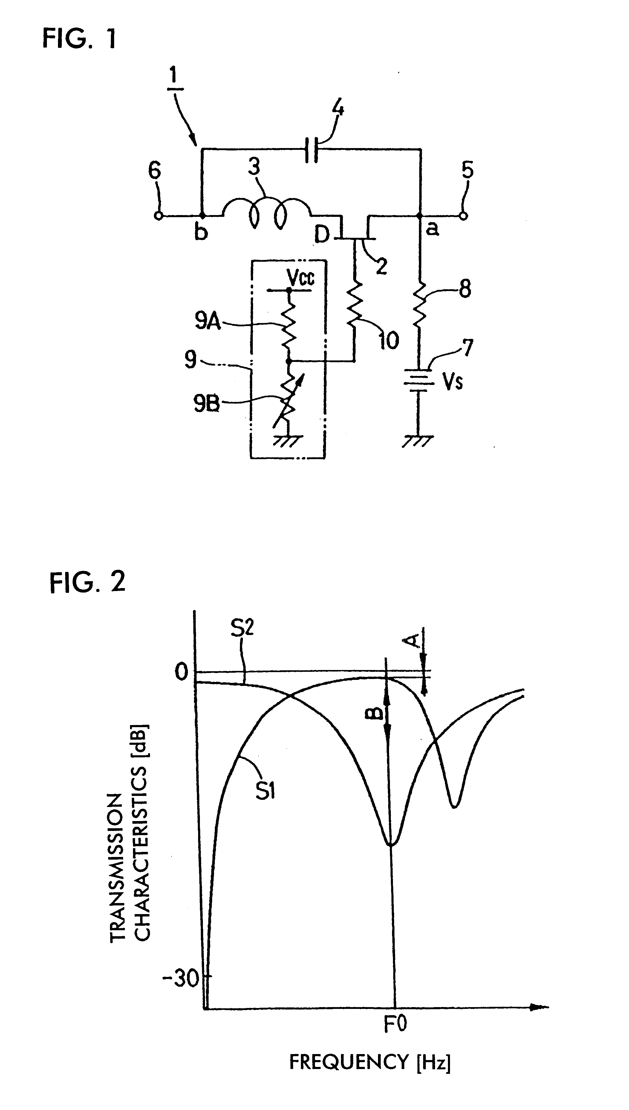
FIG. 1 and FIG. 2 illustrate an SPST switch into which a variable attenuator of the present invention is incorporated.
As shown, an SPST switch 1 includes an FET 2 later discussed, an inductive element 3, and a capacitive element 4.
The FET 2, making or breaking the circuit of the SPST switch 1, is configured with the drain thereof connected in series with the inductive element 3 discussed later and with the gate thereof connected to a variable-voltage generator 9. The FET 2 has a small resistance Ron during an on operation thereof and an off capacitance Coff during an off operation thereof. As for the terminals of the FET 2 as shown in FIG. 1, the drain only is labeled D, and the source and gate of the FET 2 are not labeled, and the same is true of FIG. 3 and other drawings.
The inductive element 3, connected in series with the FET 2, is configured with one end thereof connected to the drain of the FET 2 and with the other end thereof connected to the capacitive element 4. The inducti...
second embodiment
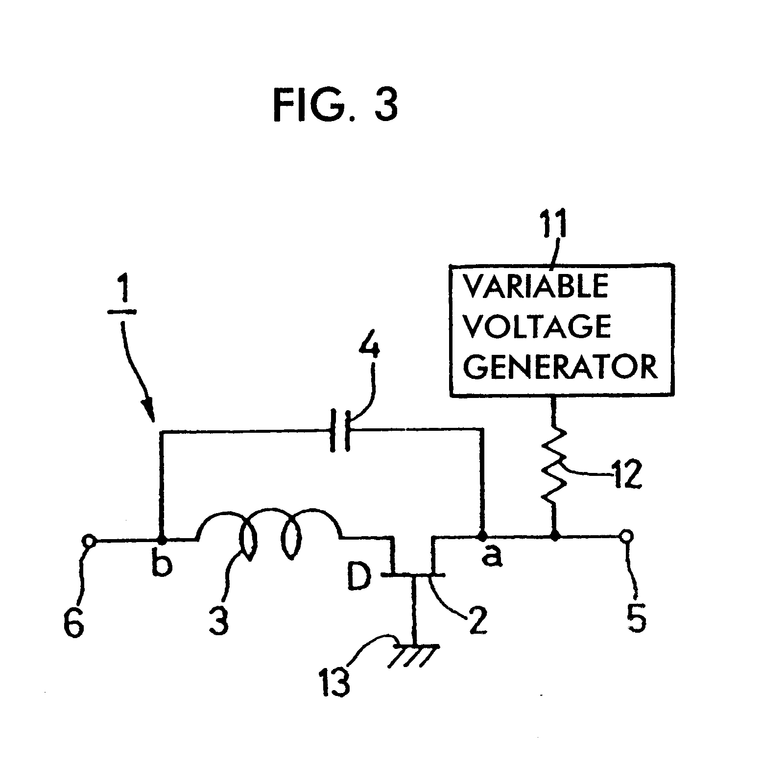
In the second embodiment, the gate of the FET 2 is connected to a ground 13. In this way, the gate of the FET 2 is maintained at the ground voltage.
The variable attenuator of the second embodiment provides the same advantages as those of the first embodiment. Since the FET 2 is configured with the gate thereof connected to the ground 13 and with the source thereof connected to the variable-voltage generator 11, the variable-voltage generator 11 feeds, to the source of the FET 2, the voltage V.alpha. or the ground voltage, thereby varying the voltage difference (the gate voltage) between the gate and source of the FET 2, and thereby switching the FET 2 between the off state and the on state. In comparison with the first embodiment, the second embodiment is simple in structure and involves low manufacturing costs because only the source of the FET 2 is biased.
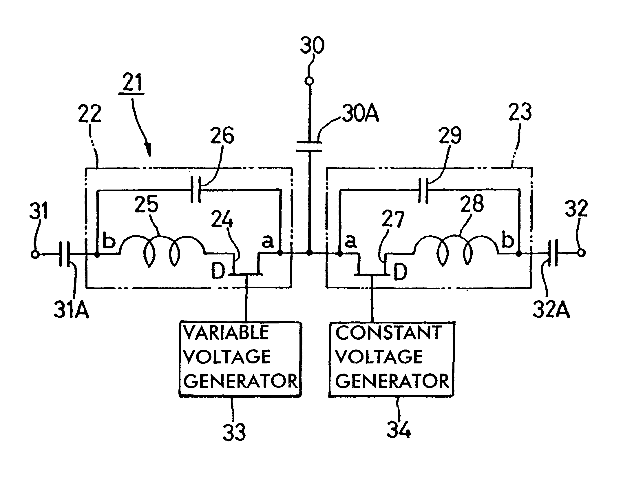
FIG. 4 illustrates a variable attenuator of a third embodiment of the present invention, and the feature of the third embodimen...
third embodiment
The SPDT switch 21 of the third embodiment is constructed as above, and the operation thereof is discussed below referring to Table 1.
To close the SPST switch 22 and to open the SPST switch 23, the variable-voltage generator 33 feeds, to the gate of the first FET 24, the voltage V.alpha. in the vicinity of the pinchoff voltage of the first FET 24, and the constant-voltage generator 34 feeds the ground voltage to the second FET 27. The first FET 24 becomes almost non-conductive, thereby causing the first inductive element 25 and the off capacitance Coff1 of the first FET 24 to resonate serially at a signal frequency, and the second FET 27 is turned on, thereby causing the second inductive element 28 and the capacitive element 29 to resonate in parallel at a signal frequency. Thus, the impedance between the first and second terminals 30 and 31 drops to almost zero, thereby closing the SPST switch 22, and the impedance between the first and third terminals 30 and 32 reaches almost infi...
PUM
 Abstract
Description
Claims
Application Information


