
Particular type of a thin layer inorganic light emitting device

a technology of inorganic light and particulate layer, which is applied in the direction of discharge tube/lamp details, discharge tube luminescent screens, discharge tubes/lamp details, etc., can solve the problem of low yield, low concentration of zns:cu dispersion in the fabrication of this device, and cannot be recommended for use. , to achieve the effect of easy manufacturing

Inactive Publication Date: 2004-04-20
AGFA GEVAERT AG
View PDF11 Cites 29 Cited by
  • Summary
  • Abstract
  • Description
  • Claims
  • Application Information

AI Technical Summary

Benefits of technology

It is an object of the present invention to provide a Thin Layer Inorganic Light Emitting Device based on zinc sulfide, which is easy to manufacture.
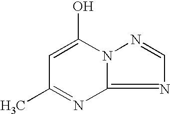
The use of diazoles and triazoles enables a better control on particle size (growth inhibitor), particle size distribution and dispersion homogenity. However, the exact working mechanism of the product during synthesis of the nano-particles is not yet completely understood. As will be illustrated furtheron, ILEDs incorporating a coated layer containing ZnS nanoparticles precipitated in the presence of 5-methyl-1,2,4-triazolo-(1,5-a)-pyrimidine-7-ol show a better neutral white electroluminescence spectrum.
In order to prepare the dispersion for coating a binder is usually added. Preferred binders are aqueous solutions of polyvinyl alcohol (PVA), polyvinyl pyrrolidone (PVP). Adding of these binders improves the stability of the nanoparticle dispersions.
The application of electroactive organic and / or inorganic materials in devices (light emitting diodes, photovoltaic cells) often requires electrodes with a difference in their respective work functions. The work function of a metal is defined as minus the energy of an electron in the Fermi level of the compact metal. The difference in work function of the electrodes creates an electric field which generally facilitates charge injection in the case of light emitting devices or charge drain off in the case of photovoltaic devices. Usually Indium Tin Oxide (ITO) is used as transparent electrode having a work-function of 4.8-4.4 eV. The high work function enables the transport of positive charges (holes). An alternative for ITO is the high conductive PEDOT / PSS coatings (ORGACON.TM., a trade mark of Agfa-Gevaert N. V.). It possesses a work function of about 5 eV and it has proven to be a valuable alternative to the ITO electrode. The ITO or PEDOT / PSS electrode is commonly used in combination with low work function metal electrodes (second conductive electrode) like Al (3-4.2 eV), Mg (2.7-3.6 eV), Ca (2.2-3.3 eV) or other alkali earth metals. For the ease of handling, Al electrodes, applied by evaporation in vacuo, are preferred. These metal electrodes enable the injection of negative charges (electrons).
In a preferred embodiment there is a so-called hole injecting layer incoporated between the first electrode and the ZnS layer. In PLED or OLED devices hole injecting layers are often applied between the ITO electrode and the electroluminescent layer. For PLEDS, PEDOT / PSS is often used. It seems that this additional layer enhances the lifetime of the devices and decreases the threshhold voltage. These beneficial effects are explained by the fact that PEDOT / PSS smoothens the ITO surface by which the number of hot spots in the operating device decreases and the work function of PEDOT / PSS is about 5.2 eV, which is 0.4 eV higher than ITO (4.8 eV) resulting in a lower barrier for hole injection and finally leading to a lower threshhold voltage. Although the argument of smoothening the ITO surface seems to be valid in some cases, another reason for improving the lifetime can be found in the effect of PSS. This compound is anionic and will therefore limit the passage of electrons by its negatively charged shielding. Electrons which will enter the ITO will recombine with the positive charges present in the ITO due to the applied bias. Because the recombination energy cannot be converted to luminescence, the energy will be converted in heat, thereby destroying the ITO electrode. Hence the lifetime of the device will be limited. It can be shown that by applying a very thin PSS layer between ITO and the electroluminescent layer holes can still be injected in the electroluminescent layer but electrons are inhibited to enter the ITO electrode. This results in a better lifetime of the devices because recombination in the ITO electrode has been decreased.

Problems solved by technology

However, the use of Cd- or Se-compounds can not be recommended due to environmental problems that can be expected.
The drawback of their system lies in the fact that the synthesis of the ZnS:Cu particles is quite cumbersome and results in low yields.
Green electroluminescence could be observed in both bias directions at 5 V. The drawback of the fabrication of this device is the low concentrations of the ZnS:Cu dispersion that can be obtained (ca 10.sup.-3 M).
Also a drawback could be the solvent based spincoating dispersion.
However, due to the differences found in the operating lifetimes of the emitting polymers, the white color will not be stable due to the faster decay of one of the emitting polymers: the emitted light will become colored.
This is also the main reason why full-color OLED or PLED displays are not yet commercial available.

Method used


Image

  • Particular type of a thin layer inorganic light emitting device
  • Particular type of a thin layer inorganic light emitting device
  • Particular type of a thin layer inorganic light emitting device

Examples


Embodiment Construction

Preparation of the ZnS Dispersion 1

The following solutions were prepared:

The ZnS dispersion was prepared as follows:

To solution 3, held at room temperature and stirred at 1500 rpm, solutions 1 and 2 were added simultaneously both at room temperature at a flow rate of 500 ml / min.

To 1000 ml of the resulting dispersion, 1000 ml of a 1% polyphosphoric acid solution was added and the dispersion was concentrated to 1000 ml by means of a Fresenius F60 cartridge. This dispersion was subsequently diafiltrated by using 5500 ml of a 1% solution of polyphosphoric acid solution in water. The dispersion was further concentrated to a volume of about 570 ml. This is dispersion 1.

Preparation of ZnS Dispersion 2

The following solution was prepared:

The ZnS dispersion was prepared as follows:

To solution 4, held at room temperature and stirred at 1500 rpm, solutions 1 and 2 were added simultaneously both at room temperature at a flow rate of 500 ml / min.

To 1000 ml of the resulting dispersion, 1000 ml of a...


PUM

PropertyMeasurementUnit
wavelengthaaaaaaaaaa
particle sizeaaaaaaaaaa

Abstract

A Thin Layer Inorganic Light Emitting device is disclosed comprising a substrate, a first electrode, a coated layer comprising substantially undoped zinc sulfide nanoparticles, and a second electrode. On applying a voltage between the two electrodes the device emits light with an emission maximum of electroluminescence at a wavelength above 450 nm.

Description

The present invention relates to a particular type of the Inorganic Light Emitting Devices based on zinc sulfide.ZnS is a well-known phosphor material. It is used in many applications like after-glow phosphors, photon conversion phosphors and electroluminescent phosphors (Cathode Ray Tube displays, Field Emission Displays, Powder Electroluminescent devices, . . . ).Back in 1928, Lenard.sup.(1) and his group found that incorporation of certain metal impurities such as Cu, Ag or Pb leads to luminescence characteristics of these ions. For this reason he called such an impurity an "activator". He also found that ZnS without these impurities can show blue luminescence if fired with alkali halide flux. This was called "self-activated" luminescence. It was later clarified that self-activated luminescence is actually activated by pairs of a halogen donor and a Zn-vacancy acceptor.Clear explanation of the luminescence centers and the mechanism of optical transitions were established in 1960s...

Claims


Application Information

Patent Timeline
Patent Type & Authority Patents(United States)
IPC IPC(8): C09K11/02C09K11/56H05B33/26H05B33/14H01L33/00H01L33/08H01L33/18H01L33/28
CPCC09K11/025C09K11/565H05B33/14H05B33/26H01L33/08H01L33/18H01L33/28
Inventor ANDRIESSEN, HIERONYMUS
Owner AGFA GEVAERT AG
Learn More