Electronic device and method for driving the same

a technology of electronic devices and driving devices, applied in the direction of identification means, instruments, television systems, etc., can solve the problems of inability to use liquid crystal display devices, liquid crystal material undergoes a significant aging deterioration in terms of resistance, and is easy to be ionized

Inactive Publication Date: 2004-04-20
SHARP KK
View PDF4 Cites 54 Cited by
  • Summary
  • Abstract
  • Description
  • Claims
  • Application Information

AI Technical Summary

Problems solved by technology

First, when using a liquid crystal material having a large (specific) dielectric anisotropy .DELTA..epsilon.(=.epsilon. / / -.epsilon..perp.) in order to reduce the threshold voltage of the liquid crystal layer, the signal voltage dependence of a feed through voltage increases, whereby it is necessary to make a correction according to the magnitude of the signal voltage. When a liquid crystal material having a large (specific) dielectric anisotropy .epsilon. / / in the long axis direction of liquid crystal molecules is used as a liquid crystal material having a large (specific) dielectric anisotropy .DELTA..epsilon., the liquid crystal capacitance is large, thereby increasing the size of TFTs (thin film transistors) for charging and increasing the load capacitance of the liquid crystal panel. Moreover, since the average dielectric constant of such a liquid crystal material is large, an impurity in the liquid crystal layer is easily ionized. Therefore, such a liquid crystal material undergoes a significant aging deterioration in terms of resistance, and thus cannot be used in a liquid crystal display device that is to be used under severe environments.
When the voltage for a gray level that requires the highest voltage is set to be lower than the normal voltage therefor, the contrast ratio is reduced, thereby reducing the display quality.
Particularly, a liquid crystal display device that displays images in a normally white mode undergoes a significant reduction in the contrast ratio and thus a significant reduction in the display quality.

Method used


Image

  • Electronic device and method for driving the same
  • Electronic device and method for driving the same
  • Electronic device and method for driving the same

Examples


embodiment 1

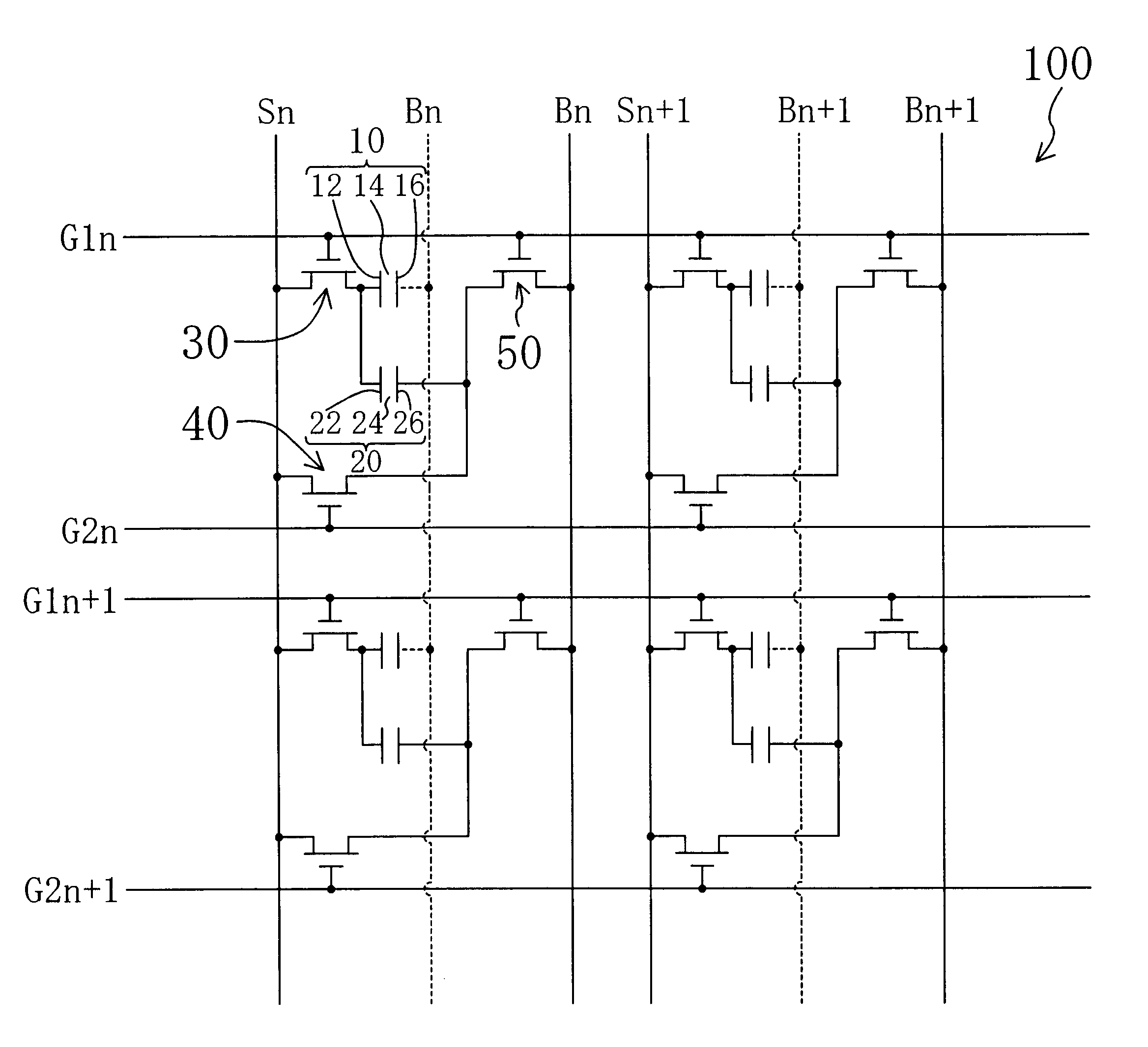
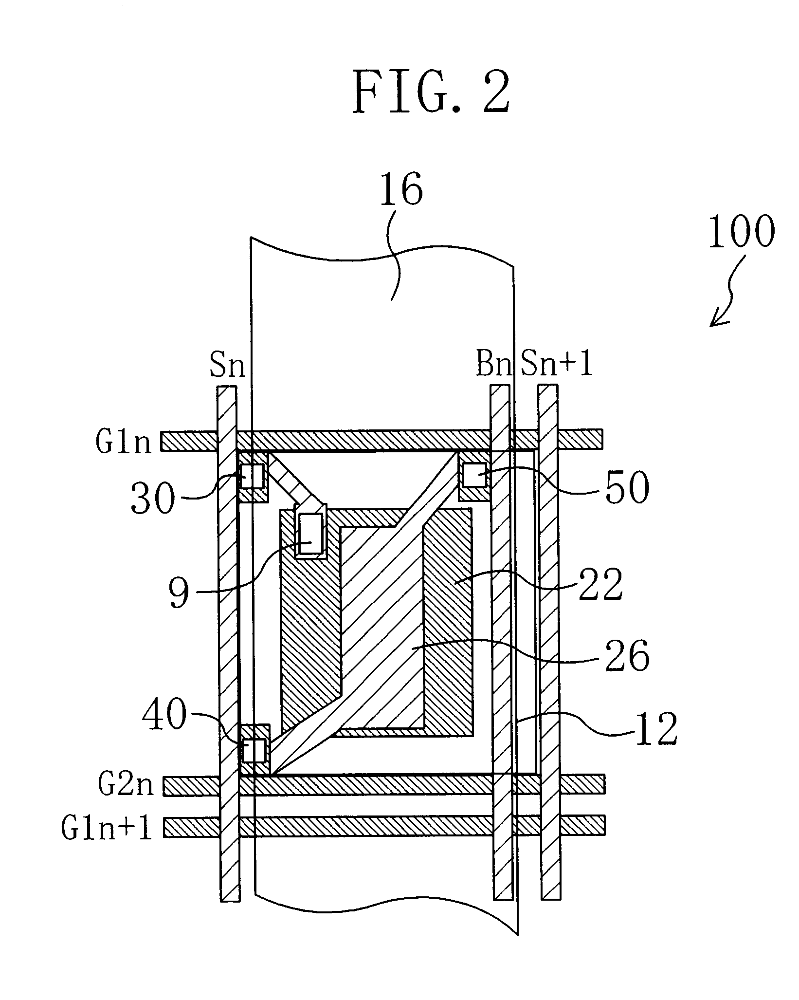
A liquid crystal display device 100, which is an electronic device of the present invention, will now be described with reference to FIG. 1. FIG. 1 is a diagram illustrating an equivalent circuit of the liquid crystal display device 100. As illustrated in FIG. 1, the liquid crystal display device 100 includes a plurality of liquid crystal capacitors 10 arranged in a matrix pattern having rows and columns, and a plurality of storage capacitors 20 corresponding respectively to the plurality of liquid crystal capacitors 10. Note that FIG. 1 only shows pixels of two rows and two columns (pixels at nth row-nth column, n.sup.th row-n+1.sup.th column, n+1.sup.th row-n.sup.th column and n+1.sup.th row-n+1.sup.th column) among a plurality of pixels respectively including the plurality of liquid crystal capacitors 10 arranged in a matrix pattern.

Each of the plurality of liquid crystal capacitors 10 includes a pixel electrode 12, a counter electrode 16 opposing the pixel electrode 12, and a l...

embodiment 2

A liquid crystal display device 200, which is an electronic device according to Embodiment 2 of the present invention, will now be described with reference to FIG. 7 and FIG. 8. FIG. 7 is a diagram illustrating an equivalent circuit of the liquid crystal display device 200, and FIG. 8 is a top view schematically illustrating a portion of the liquid crystal display device 200 corresponding to one pixel. The liquid crystal display device 200 will be described below while focusing on the differences thereof from the liquid crystal display device 100 of Embodiment 1. Elements having substantially the same functions as those of the liquid crystal display device 100 will be denoted by the same reference numerals and will not be further discussed below.

The liquid crystal display device 200 includes a plurality of additional storage capacitors 60 corresponding respectively to the plurality of liquid crystal capacitors 10. Each storage capacitor 60 includes an additional storage capacitor el...

embodiment 3

A liquid crystal display device 300, which is an electronic device according to Embodiment 3 of the present invention, will now be described with reference to FIG. 9 and FIG. 10. FIG. 9 is a diagram illustrating an equivalent circuit of the liquid crystal display device 300, and FIG. 10 is a top view schematically illustrating a portion of the liquid crystal display device 300 corresponding to one pixel.

The liquid crystal display device 300 includes a single counter electrode (e.g., an ITO layer) 16' provided substantially across the entire surface of the counter substrate as illustrated in FIG. 10. The TFT substrate of the liquid crystal display device 300 includes a reference line B provided for each column so as to cross the signal line Si, as illustrated in FIG. 9 and FIG. 10, and the reference line B is electrically connected to the counter electrode 16' at a common transfer section provided outside the display area.

The reference line B is formed by patterning the same metal la...


PUM

PropertyMeasurementUnit
voltageaaaaaaaaaa
conductivityaaaaaaaaaa
voltageaaaaaaaaaa

Abstract

An electronic device includes on a substrate: a plurality of first capacitors each including a first electrode and a second electrode opposing the first electrode via a first dielectric layer; a plurality of second capacitors each including a third electrode electrically connected to the first electrode and a fourth electrode opposing the third electrode via a second dielectric layer; a first line whose electrical connection to the first electrode and the third electrode is turned ON / OFF by a first switching element; a second line electrically connected to the second electrode at least temporarily; a third line whose electrical connection to the fourth electrode is turned ON / OFF by a second switching element; and a fourth line whose electrical connection to the fourth electrode is turned ON / OFF by a third switching element.

Description

1. Field of the InventionThe present invention relates to an electronic device and a method for driving the same.2. Description of the Background ArtIn recent years, flat display panels have been used as display devices in a display unit of a notebook computer, a portable telephone, or a personal digital assistant (PDA). Many of such flat display panels are liquid crystal display devices. Since the power consumption is one of the factors that determine the product value of these portable devices, there is a demand for reducing the power consumption of a liquid crystal display device used in a display unit. Particularly, there is a demand for reducing the power consumption of the liquid crystal module itself in order to further reduce the power consumption of a reflection type liquid crystal display device that has no backlight.Typically, the power consumption Pw of an electronic device including many capacitors such as a liquid crystal display device is expressed as Pw=C.multidot.f....

Claims


Application Information

Patent Timeline
Patent Type & Authority Patents(United States)
IPC IPC(8): G09G3/36G02F1/1368G02F1/133G09F9/30G09G3/20H04N5/66
CPCG09G3/3659G09G2300/0842
Inventor YAMAMOTO, TOMOHIKOTANAKA, KEIICHIICHIOKA, HIDEKIINOUE, NAOTOFUJIWARA, KOJI
Owner SHARP KK
Why Eureka
Try Eureka