Methods and apparatus for holding and positioning semiconductor workpieces during electropolishing and/or electroplating of the workpieces

a technology for workpieces and semiconductors, applied in the direction of electrochemical machining apparatus, supporters, surface reaction electrolytic coatings, etc., can solve the problems of increasing increasing the signal delay at the interconnection, and developing more powerful semiconductor devices

Inactive Publication Date: 2004-04-27
ACM RES
View PDF7 Cites 128 Cited by
  • Summary
  • Abstract
  • Description
  • Claims
  • Application Information

AI Technical Summary

Problems solved by technology

However, one potential limiting factor to developing more powerful semiconductor devices is the increasing signal delays at the interconnections (the lines of conductors, which connect elements of a single semiconductor device and / or connect any number of semiconductor devices together).
However, the closer proximity of interconnections increases the line-to-line capacitance of the interconnections, which results in greater signal delay at the interconnections.
However, this approach has the disadvantage of increasing production costs associated with forming the additional layers of metal.
Furthermore, these additional layers of metal generate additional heat, which can be adverse to both chip performance and reliability.
Also, copper is less resistant to electromigration (meaning that a line formed from copper will have less tendency to thin under current load) than aluminum.

Method used


Image

  • Methods and apparatus for holding and positioning semiconductor workpieces during electropolishing and/or electroplating of the workpieces
  • Methods and apparatus for holding and positioning semiconductor workpieces during electropolishing and/or electroplating of the workpieces
  • Methods and apparatus for holding and positioning semiconductor workpieces during electropolishing and/or electroplating of the workpieces

Examples


Embodiment Construction

In order to provide a more thorough understanding of the present invention, the following description sets forth numerous specific details, such as specific material, parameters, and the like. It should be recognized, however, that such description is not intended as a limitation on the scope of the present invention, but is instead provided to enable a more full and a more complete description of the exemplary embodiments.

Additionally, the subject matter of the present invention is particularly suited for use in connection with electroplating and / or electropolishing of semiconductor workpieces or wafers. As a result, exemplary embodiments of the present invention are described in that context. It should be recognized, however, that such description is not intended as a limitation on the use or applicability of the present invention. Rather, such description is provided to enable a more full and a more complete description of the exemplary embodiments.

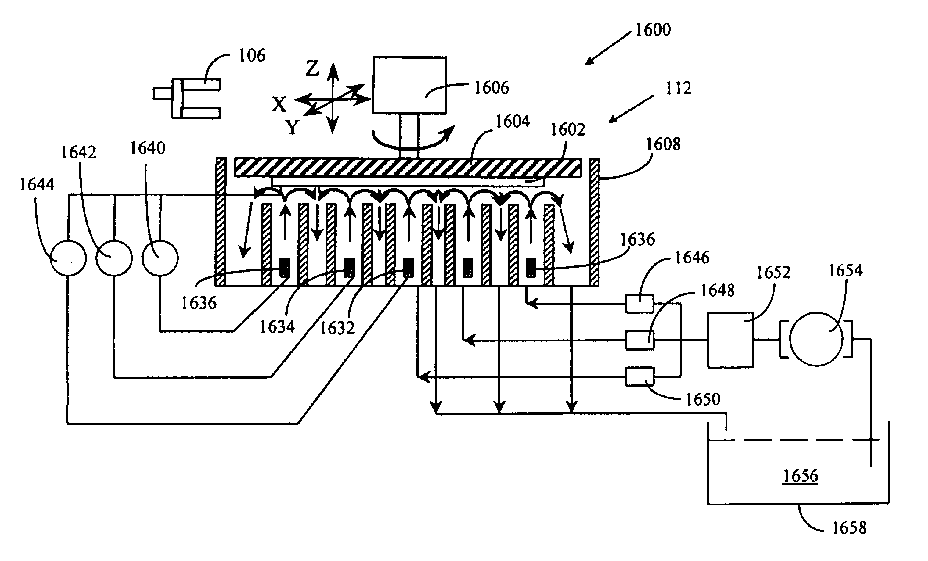
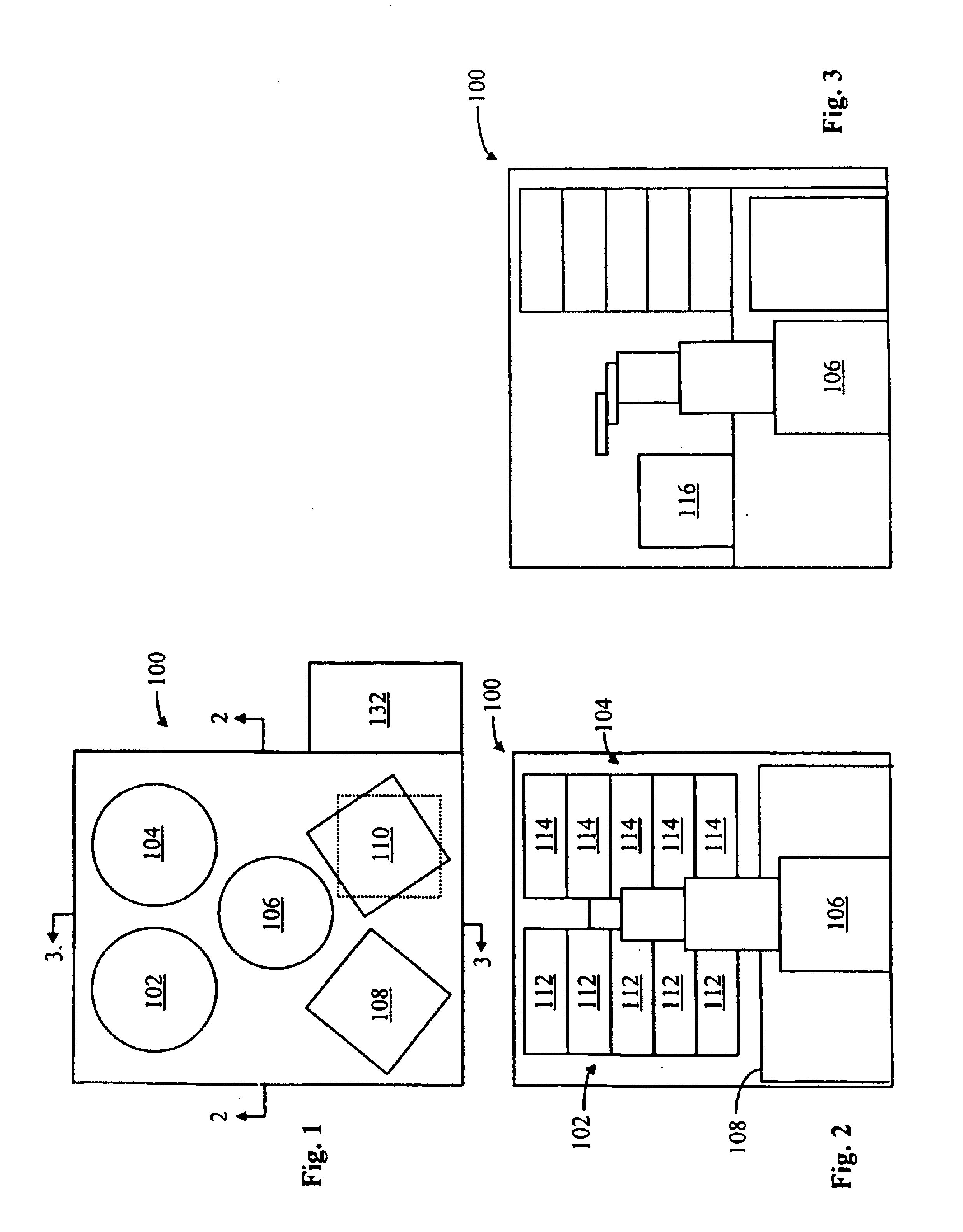
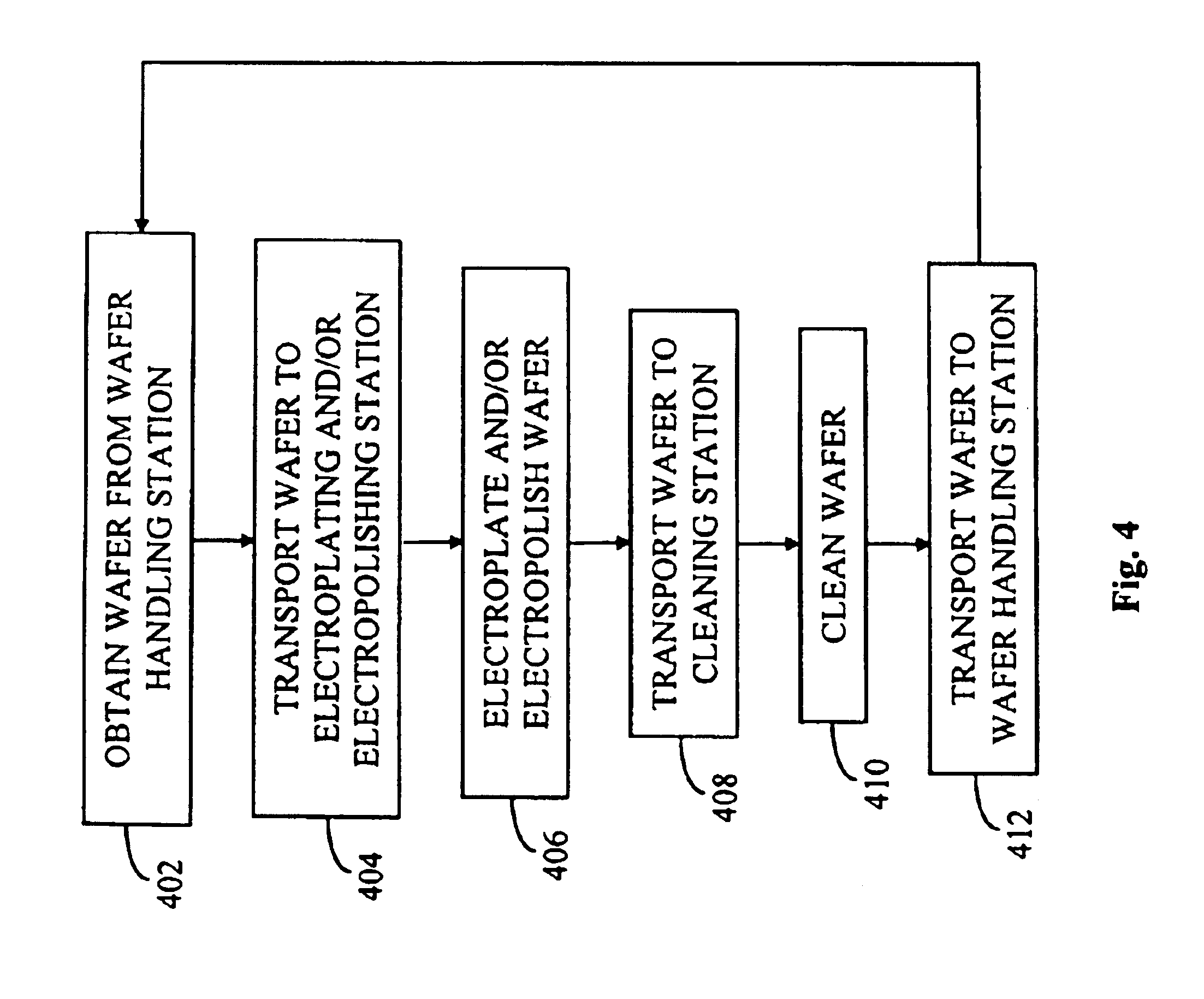
With reference now to FIG. 1, a...


PUM

PropertyMeasurementUnit
feature sizeaaaaaaaaaa
surface roughnessaaaaaaaaaa

Abstract

A wafer chuck assembly for holding a wafer during electroplating and/or electropolishing of the wafer includes a wafer chuck for receiving the wafer. The wafer chuck assembly also includes an actuator assembly for moving the wafer chuck between a first and a second position. When in the first position, the wafer chuck is opened. When in the second position, the wafer chuck is closed.

Description

1. Field of the InventionThe present invention generally relates to methods and apparatus for holding and positioning semiconductor workpieces during processing of the workpieces. More particularly, the present invention relates to methods and apparatus for holding and positioning semiconductor workpieces during electroplating and / or electropolishing of semiconductor workpieces.2. Description of the Related ArtIn general, semiconductor devices are manufactured or fabricated on disks of semiconducting materials called wafers or slices. More particularly, wafers are initially sliced from a silicon ingot. The wafers then undergo multiple masking, etching, and deposition processes to form the electronic circuitry of semiconductor devices.During the past decades, the semiconductor industry has increased the power of semiconductor devices in accordance with Moore's law, which predicts that the power of semiconductor devices will double every 18 months. This increase in the power of semico...

Claims


Application Information

Patent Timeline
Patent Type & Authority Patents(United States)
IPC IPC(8): H01L21/687H01L21/00H01L21/02H01L21/288H01L21/67H01L21/321B23H5/08C25D5/00C25D5/02C25D7/12C25D17/00C25D17/04C25D17/06C25F3/16
CPCB23H5/08C25D17/06C25D17/001C25D7/123
Inventor WANG, HUIGUTMAN, FELIXNUCH, VOHA
Owner ACM RES
Why Eureka
Try Eureka