

Method for forming low-dielectric constant film on semiconductor substrate by plasma reaction using high-RF power
a technology of plasma reaction and semiconductor substrate, applied in the field of semiconductor technology, can solve the problems of affecting high-speed operations, affecting the hardness of the film, and affecting the capacitance of individual wires
- Summary
- Abstract
- Description
- Claims
- Application Information
AI Technical Summary
Benefits of technology
Problems solved by technology
Method used
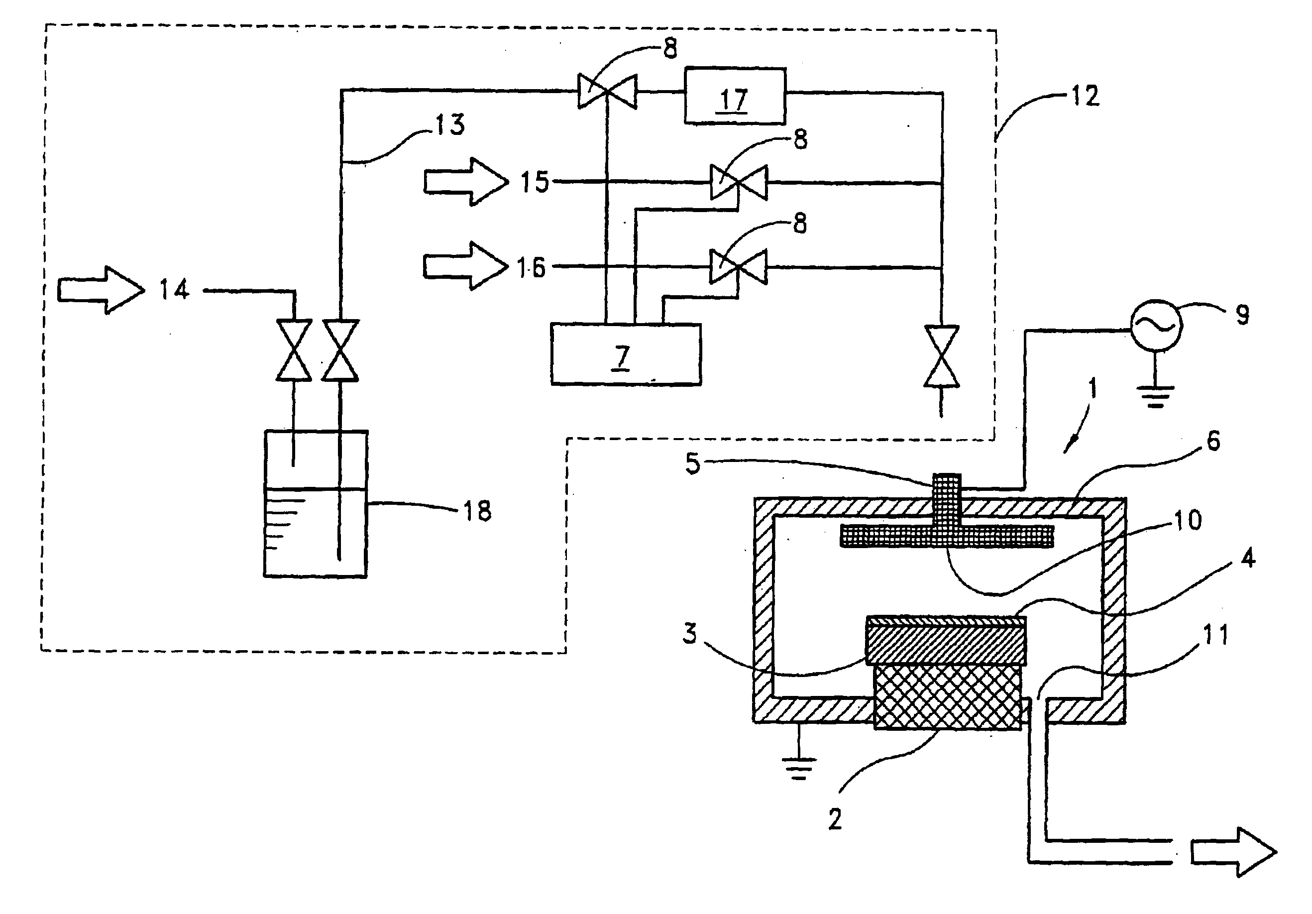
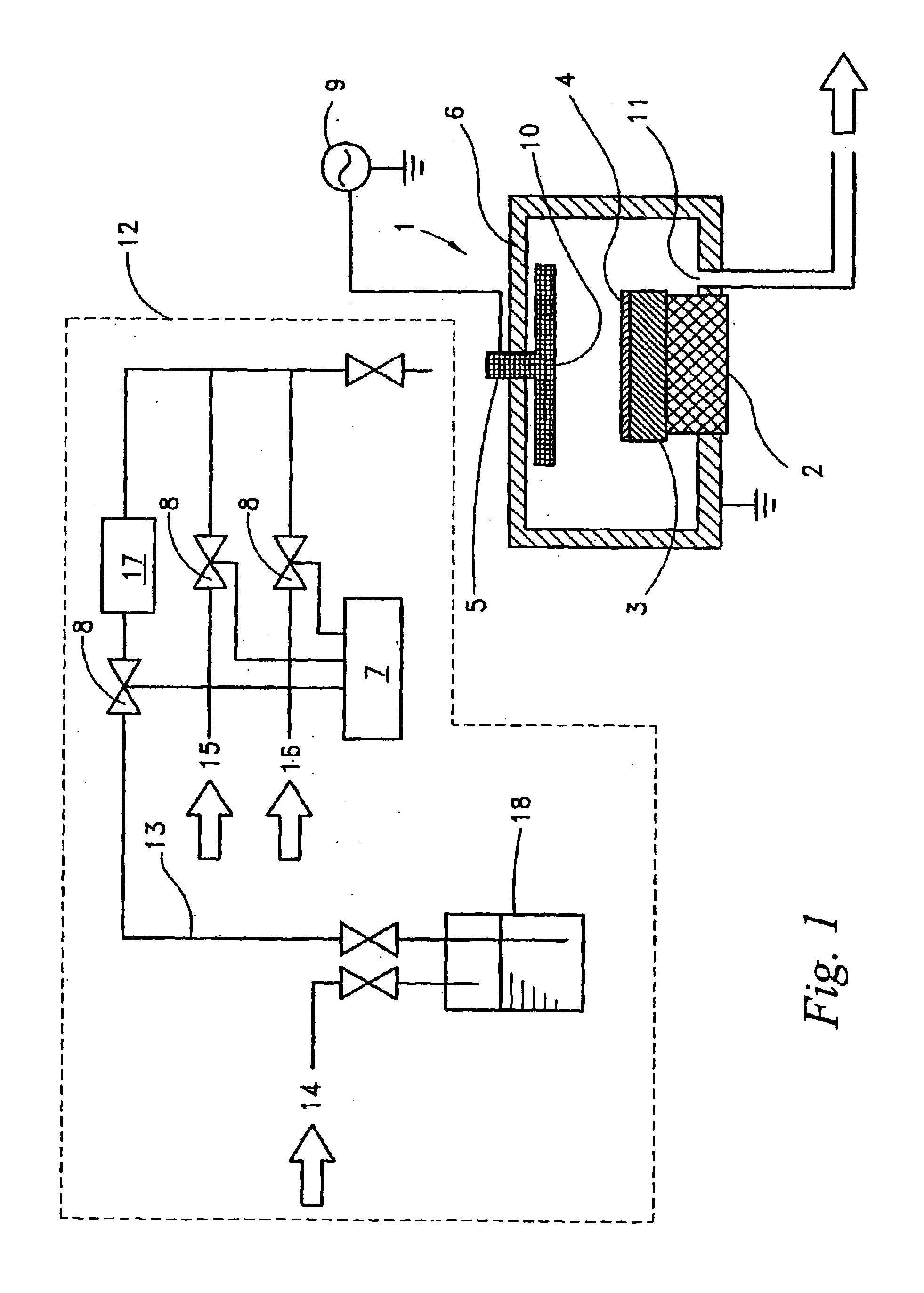
Image

Examples
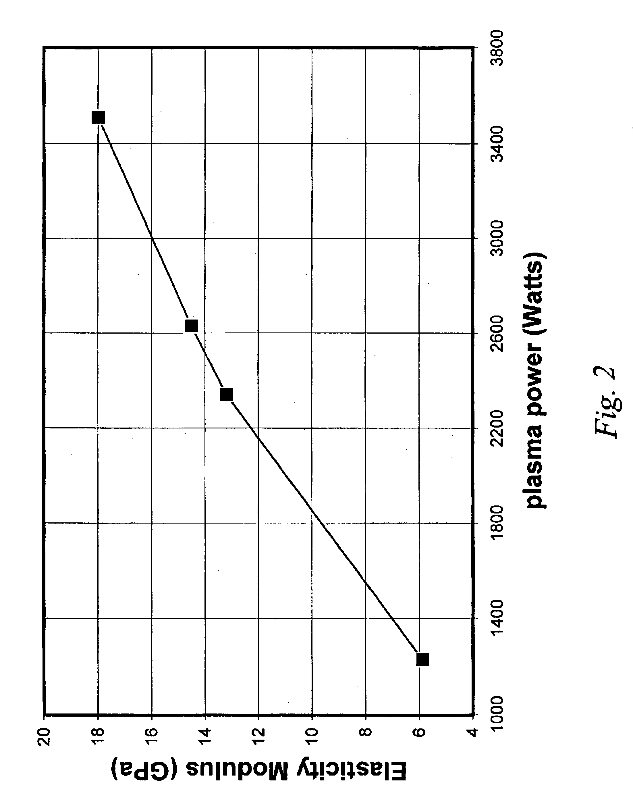
experiment 1
In Experiment 1, as shown in Table 1-1, substrates having a diameter of 200 mm were used, and no additive gas was used. In Experiment 2, as shown in Table 2-1, substrates having a diameter of 300 mm were used, and as an additive gas, 1,2-propanediol was added at 200 sccm. In Experiment 3, as shown in Table 3-1, substrates having a diameter of 300 mm was used, and as an additive gas, oxygen was added at 100 sccm.
TABLE 1-2
TABLE 2-1
TABLE 2-2
TABLE 3-1
TABLE 3-2
As shown in the tables, when the RF power is high (over 1,500 W, further over 2,000 W) under a relatively high pressure, the hardness and the elasticity modulus of the resultant films become significantly high without significant increases of the dielectric constant. Further, when a cross-linker gas or an oxidizing gas (especially a cross-linker gas) is added, the mechanical strength further increases. Also, FIGS. 2 and 3 show the results of Experiments 2.4, 2.5, 2.6 and 2.7.
Although this invention has been described in terms of ce...
PUM
 Abstract
Description
Claims
Application Information