Active matrix type liquid crystal display device having particular positioning reference pattern and fabrication method thereof

a liquid crystal display and active matrix technology, applied in the direction of identification means, instruments, optics, etc., can solve the problems of unfavorable lateral alignment, uneven display of division, and high cost of photo masks

Inactive Publication Date: 2004-06-01
BEIHAI HKC OPTOELECTRONICS TECH CO LTD
View PDF8 Cites 40 Cited by
  • Summary
  • Abstract
  • Description
  • Claims
  • Application Information

AI Technical Summary

Problems solved by technology

Since, when the size of a liquid crystal panel becomes larger, the size of the photo mask for transferring a pattern of a liquid crystal panel onto a whole surface of the substrate becomes larger, the cost of the photo mask becomes very high.
When the overlapped area between the adjacent exposure shots is large, the quality of formed pattern becomes different between the exposure shots, resulting in a display defect called unevenness of division.
Therefore, there is a problem that it is impossible to precisely perform the lateral alignment and unevenness of division tends to occur.
Further, liquid crystal may erroneously operate by electric field of the scanning line 28.
Further, when the interlayer insulating film is constructed with a single organic film, an interface between the semiconductor layer of the TFT and the organic film covering the semiconductor layer becomes unstable and, when it is driven at high temperature, leak current of the TFT is increased, causing display variation.
Therefore, it is impossible to perform the lateral alignment precisely and the divisional variation tends to occur.

Method used


Image

  • Active matrix type liquid crystal display device having particular positioning reference pattern and fabrication method thereof
  • Active matrix type liquid crystal display device having particular positioning reference pattern and fabrication method thereof
  • Active matrix type liquid crystal display device having particular positioning reference pattern and fabrication method thereof

Examples


first embodiment

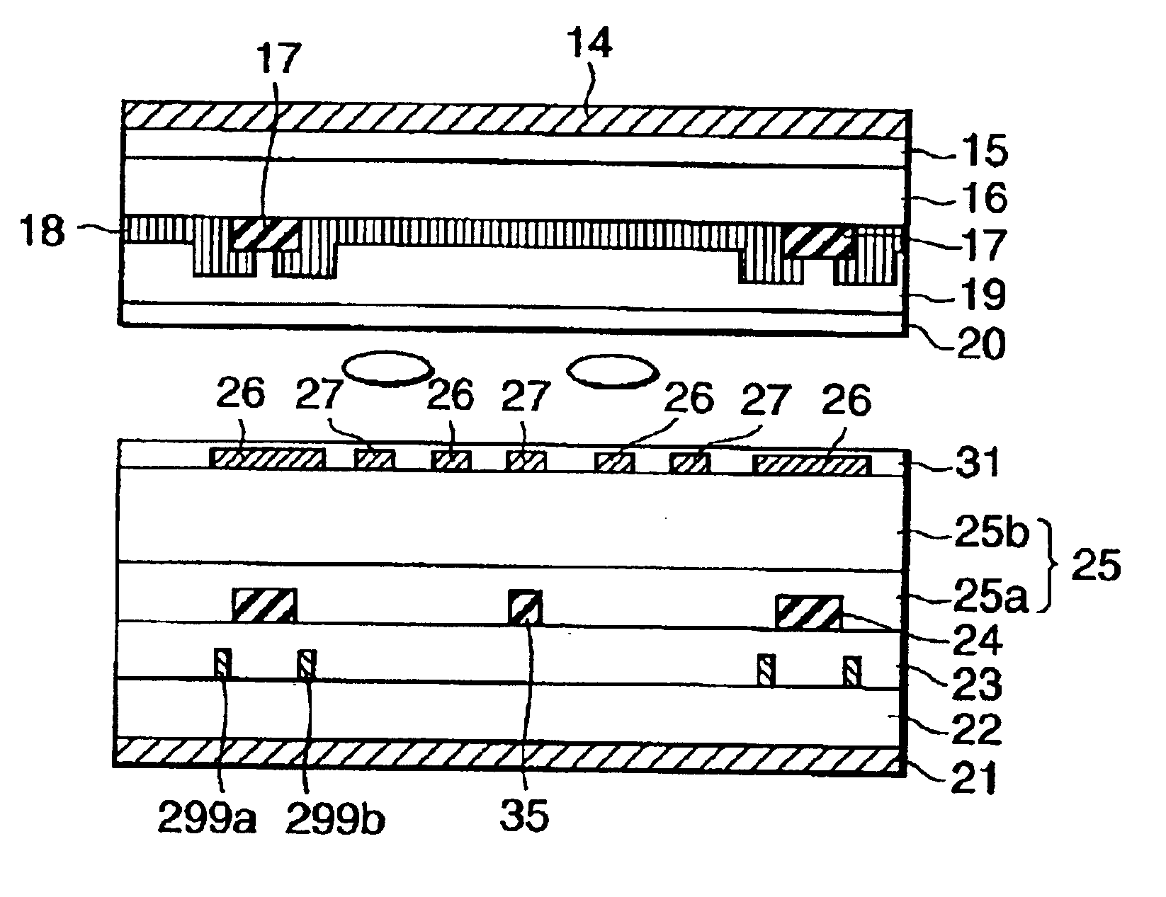
In a first embodiment, the second interlayer insulating film 25 is a lamination of the inorganic film and an organic film.

As shown in FIG. 18A, the gate electrode 30c and the common electrode wiring portions 26a and 26b are formed by patterning the first metal layer formed of chromium on the transparent insulating substrate 22 of glass by photolithography and dry etching. Although only the common electrode wiring portion 26b is shown in FIG. 18A to FIG. 18K, the common electrode wiring portion 26a, which is inevitable, will be described together in the following description.

The photolithography is performed by depositing a film to be patterned on a whole surface of the transparent insulating substrate 22, forming a photosensitive resin film on the whole surface of the deposited film by spin coating, exposing the photosensitive resin film with light having a specific wavelength with which the photosensitive organic film is hardened by using a photo mask shielding only a desired patte...

second embodiment

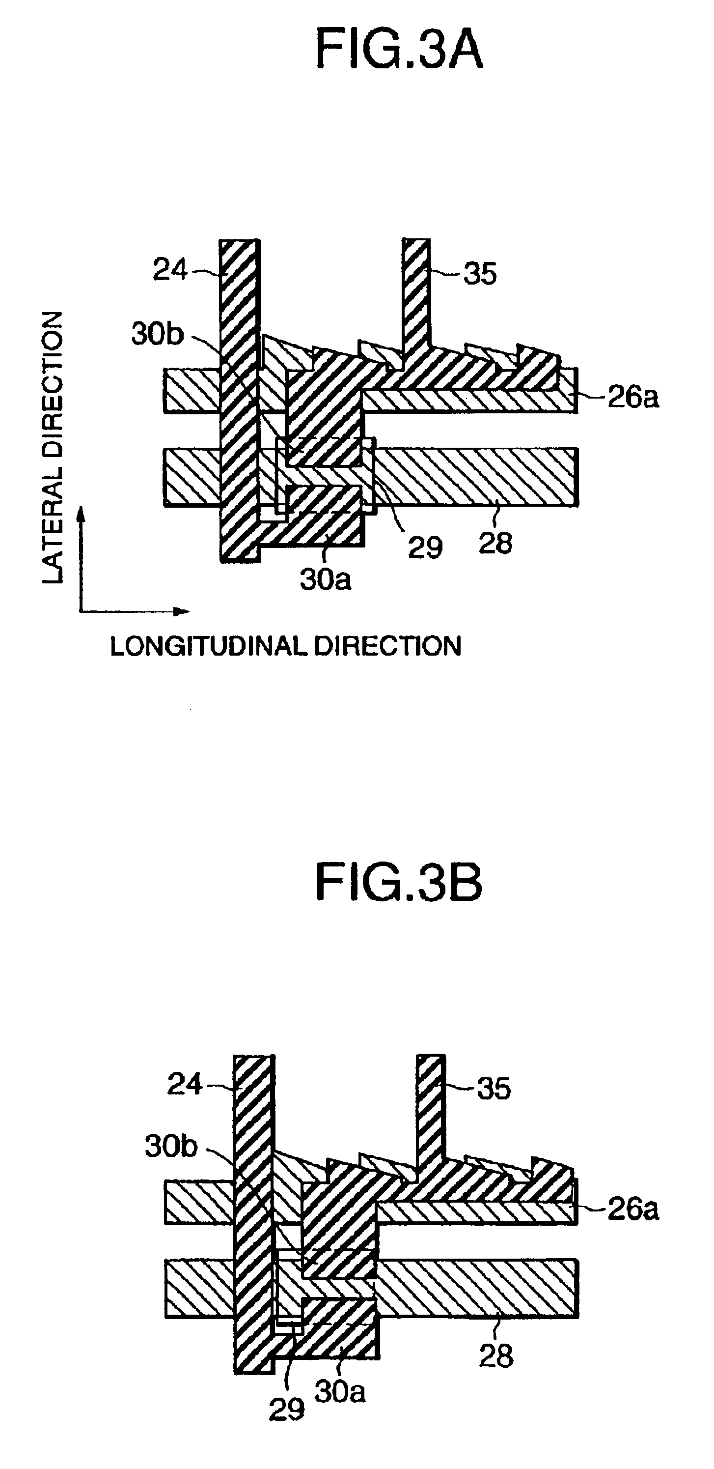
FIG. 21A and FIG. 21B shows the second embodiment, which are basically the same as FIG. 10A and FIG. 10B showing the first embodiment shown in FIG. 7, which show the region formed by the first and second metal layers shown in FIG. 7 and the region formed of ITO shown in FIG. 7, respectively. A manufacturing method of the liquid crystal display device according to the second embodiment is also the same as that of the first embodiment. The second embodiment differs from the first embodiment in the configuration of the protruded portions formed in the common electrode wiring portion 26a and extending in parallel to the longitudinal direction of the data line.

Although the protruded portions 299a and 299b of the common electrode wiring 26 are arranged on both sides of the data line 24 in a plane in the first embodiment, only one protruded portion (299a) having width larger than width of the protruded portion in the first embodiment is provided adjacent to the data line as shown in FIG. 2...

third embodiment

FIG. 22A and FIG. 22B shows the second embodiment, which are basically the same as FIG. 10A and FIG. 10B showing the first embodiment shown in FIG. 7, which show the region formed by the first and second metal layers shown in FIG. 7 and the region formed of ITO shown in FIG. 7, respectively. A manufacturing method of the liquid crystal display device according to the second embodiment is also the same as that of the first embodiment. The second embodiment differs from the first embodiment in the configuration of the protruded portions formed in the common electrode wiring portion 26a and extending in parallel to the longitudinal direction of the data line.

Although the protruded portions 299a and 299b of the common electrode wiring 26 are arranged adjacently on both sides of the data line 24 in a plane in the first embodiment, a protruded portion 299a is provided adjacently on one side of the data line 24 and another protruded portion 299c is provided slightly remote from the protrud...


PUM

PropertyMeasurementUnit
widthaaaaaaaaaa
widthaaaaaaaaaa
widthaaaaaaaaaa

Abstract

In an in-plane switching (IPS) mode active matrix type liquid crystal display device, data lines 24 supplied with data signals, common electrode wiring portions 26a and 26b applied with a reference voltage, a common electrode 26, pixel electrodes corresponding to pixels to be displayed, scanning lines 28 supplied with scan signals and TFT's 50 are provided on an active element substrate 11. The common electrode wiring portions 26a and 26b are formed by using a first metal layer, extend in parallel to the scanning line and connected to a common electrode potential at a peripheral portion thereof. Protruded portions 299a and 299b are formed in at least one of the common electrode wiring portions 26a and 26b in such a way that the protruded portions are positioned on both sides of the data line 24 to be formed later. Unevenness of display of the display device is reduced and the aperture ratio thereof is improved.

Description

1. Field of the InventionThe present invention relates to a liquid crystal display device and a fabrication method thereof and, particularly, to an IPS (In-Plane Switching) mode active matrix type liquid crystal display device and a fabrication method thereof.2. Description of the Prior ArtAn active matrix type liquid crystal display device (referred to as "AMLCD", hereinafter), which uses TFT's (Thin Film Transistors) as pixel switching elements, can provide a high image quality and has been used as a display device of a portable type computer and, particularly, as a monitor of a compact desk-top computer recently.The AMLCD is roughly classified to a type in which a display is performed by rotating a direction of molecular axis of oriented liquid crystal molecule, which is called "director", in a plane orthogonal to a substrate thereof and a type in which a display is performed by rotating the director in a plane parallel to the substrate.A liquid crystal display device of the TN (...

Claims


Application Information

Patent Timeline
Patent Type & Authority Patents(United States)
IPC IPC(8): G02F1/13G02F1/1343G02F1/1335G02F1/1368G09F9/30H01L21/027H01L21/336H01L29/786
CPCG02F1/134363G02F1/1343
Inventor MATSUMOTO, KIMIKAZUHANNUKI, TAKAHISAKOIKE, MASASHINISHIDA, SHINICHIITAKURA, KUNIMASA
Owner BEIHAI HKC OPTOELECTRONICS TECH CO LTD
Why Eureka
Try Eureka