High-frequency amplifier

a high-frequency amplifier and amplifier technology, applied in amplifiers, amplifiers with semiconductor devices only, amplifiers with semiconductor devices, etc., can solve the problems of reducing and reducing saturation output power and efficiency. , to achieve the effect of high power output and high efficiency

Inactive Publication Date: 2004-06-15
MITSUBISHI ELECTRIC CORP
View PDF6 Cites 9 Cited by
  • Summary
  • Abstract
  • Description
  • Claims
  • Application Information

AI Technical Summary

Benefits of technology

With this configuration, designing a size ratio of the first and second PMOS transistors forming the current mirror so as to approximate a voltage drop to just zero, or a value infinitely close t...

Problems solved by technology

Accordingly, when the power of input signal increases, since the amplifier operation rapidly approaches to the B-class, the saturation power decreases, and the high power output and high efficiency cannot be achieved.
Accordingly, in the high frequency amplifier of the conventional technique, when the high frequency input signal Pin increases...

Method used


Image

  • High-frequency amplifier
  • High-frequency amplifier
  • High-frequency amplifier

Examples


embodiment 1

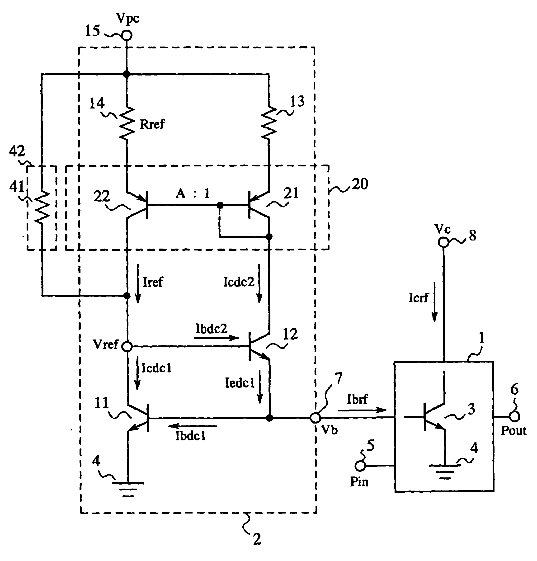
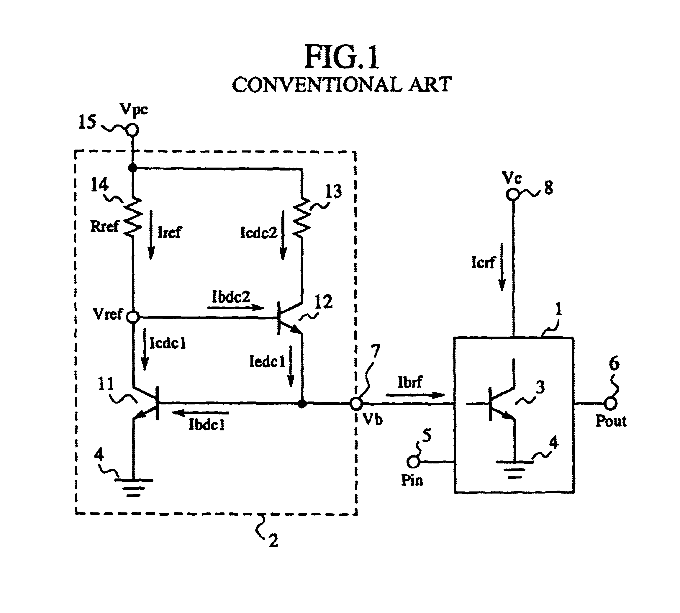
FIG. 2 is a circuit diagram illustrating a high frequency amplifying device according to the present invention, and in the figure, reference numeral 1 signifies a high frequency amplifier using an NPN bipolar transistor such as the BJT, HBT, or the like, as an amplifying element, and 2 signifies a constant voltage biasing circuit that supplies a base bias voltage to the high frequency amplifier 1.

In the high frequency amplifier 1, reference numeral 3 signifies an NPN bipolar transistor (a first NPN bipolar transistor) such as the BJT, HBT, or the like, 4 a ground connected to the emitter terminal of the NPN bipolar transistor 3, 5 a high frequency signal input terminal, 6 a high frequency signal output terminal, 7 a base bias terminal, 8 a collector bias terminal.

In the constant voltage biasing circuit 2, reference numeral 11 signifies an NPN bipolar transistor (a second NPN bipolar transistor) such as the BJT, HBT, or the like, which configures a current mirror circuit together wit...

embodiment 2

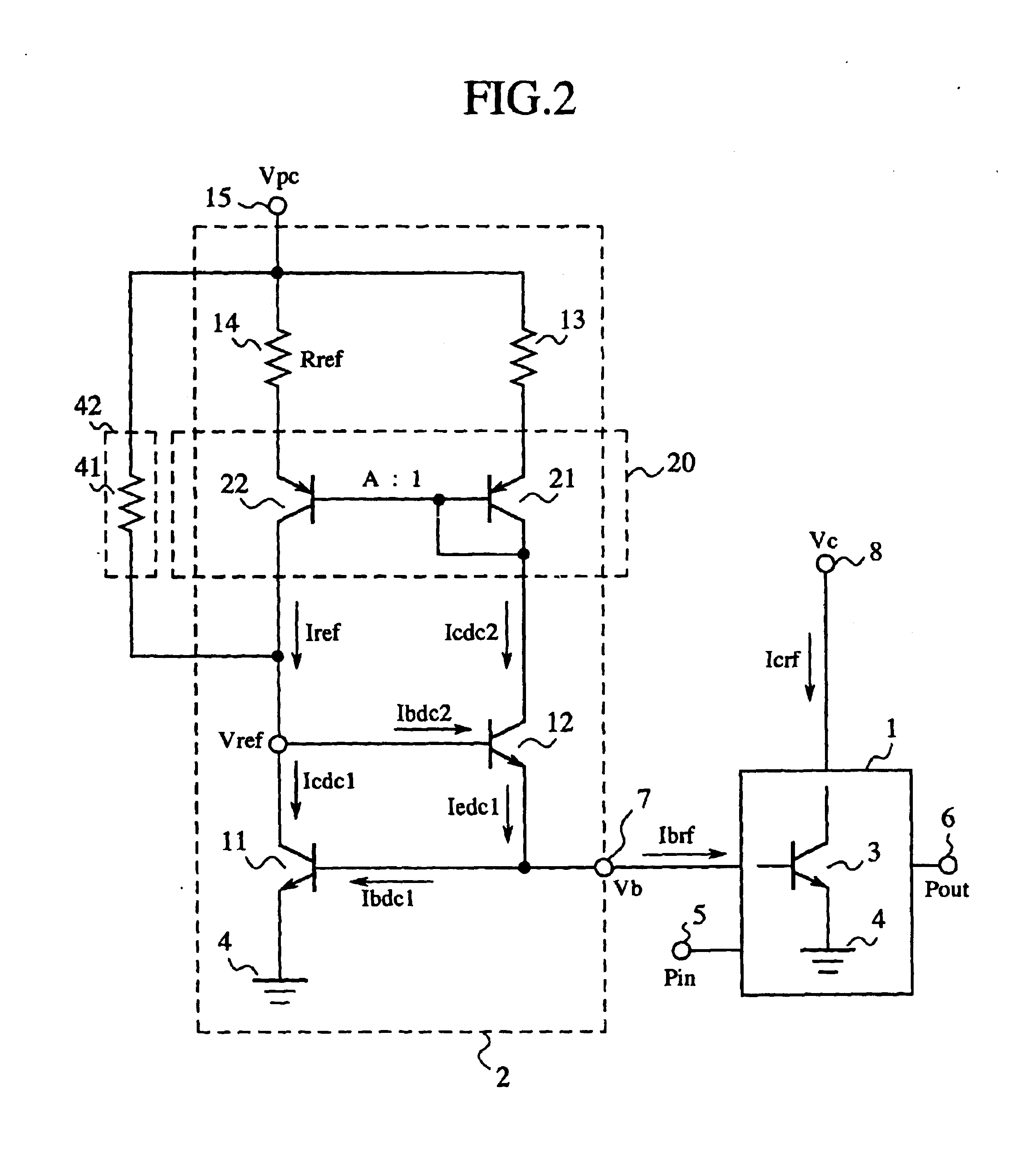
FIG. 3 is a circuit diagram illustrating a high frequency amplifying device according to the embodiment 2 of the present invention, and in the figure, reference numeral 30 signifies a current mirror that uses the collector current of an NPN bipolar transistor 12 as the reference current, and determines the collector current of an NPN bipolar transistor 11, and 31, 32 signify PMOS transistors (first and second PMOS transistors) that constitute the current mirror. In the current mirror, the gates of the PMOS transistors 31, 32 are connected to each other, the gate and drain terminals of the PMOS transistor 31 are commonly connected to the collector terminal of the NPN bipolar transistor 12, and the drain terminal of the PMOS transistor 32 is connected to the base terminal of the NPN bipolar transistor 12.

Further, the resistor (first resistor) 13 is connected between the source terminal of the PMOS transistor 31 and the power supply / voltage, setting terminal 15, the resistor (second re...


PUM


Abstract

Between resistors 13, 14 and an NPN bipolar transistor 12 are interposed PNP bipolar transistors 21, 22 forming a current mirror 20 that uses a collector current of the NPN bipolar transistor 12 as a reference current, and determines a collector current of an NPN bipolar transistor 11. This makes possible to design a size ratio A of the PNP bipolar transistors 21, 22 so as to approximate a voltage drop DeltaVb to a value close to zero, and to suppress the voltage drop DeltaVb of the base voltage Vb accordingly to achieve a high power output and high efficiency when a high frequency input signal Pin increases and generates a base rectified current.

Description

This application is the national phase under 35 U.S.C. .sctn. 371 of PCT International Application No. PCT / JP00 / 07085 which has an International filing date of Oct. 12, 2000, which designated the United States of America.The present invention relates to a high frequency amplifying device for use in a satellite communication, ground microwave communication, mobile communication, and the like.Generally, a high frequency amplifier using an NPN bipolar transistor of the BJT, HBT, or the like takes on a constant voltage biasing circuit that applies a constant voltage to the base in order to achieve a high power output and high efficiency. When a constant bias current is applied to the base, and when power of a high frequency input signal increases and generates a rectified current, the base voltage drops in order to maintain the constant current. Accordingly, when the power of input signal increases, since the amplifier operation rapidly approaches to the B-class, the saturation power de...

Claims


Application Information

Patent Timeline
IPC IPC(8): H03F3/189H03F3/343H03F1/02H03F3/19H03F1/30
CPCH03F1/0261H03F1/302H03F3/19H03F3/343H03F2201/3215
Inventor MORI, KAZUTOMISHINJO, SHINTAROUJOBA, HIROYUKITAKAHASHI, YOSHINORIIKEDA, YUKIOTAKAGI, TADASHI
Owner MITSUBISHI ELECTRIC CORP
Why Eureka
Try Eureka