Polishing head assembly

a technology of wafer carrier head and assembly, which is applied in the direction of grinding machines, manufacturing tools, lapping machines, etc., can solve the problems of uneven contact between the polishing pad and achieve the effect of optimizing the tilt and deformation effectively cancelling, and optimizing the tilt of the wafer carrier head

Inactive Publication Date: 2004-06-29
APPLIED MATERIALS INC
View PDF20 Cites 21 Cited by
  • Summary
  • Abstract
  • Description
  • Claims
  • Application Information

AI Technical Summary

Benefits of technology

In addition to transferring the loading force, the head retainer assembly is also operable to optimize the tilt and the deformation of the wafer carrier head. Optimization of the tilt of the wafer carrier head involves using a ball and socket arrangement to allow the wafer carrier head to gimbal with respect to the head retainer assembly. The determination of the optimal location of a gimbal center that effectively cancels a moment force associated with the moving polishing pad optimizes the tilt of the wafer carrier head. When the wafer on the wafer carrier head is brought into contact with the polishing pad, the moment force can cause the wafer carrier head to tilt and unevenly contact the polishing pad. By adjusting the location of the gimbal center based on testing under process conditions, the tilt of the wafer carrier head can be controlled.
The load suspension plate distributes the loading force that is transferred to the wafer carrier head. Control of the distribution of the loading force controls the deformation of the wafer carrier head. Optimization of the flatness of the wafer may be obtained by controlling the deformation of the wafer carrier head. Adjusting the diameter of the load suspension plate controls the deformation of the wafer carrier head and the wafer thereon. The load suspension plate includes a flat circular plate that contacts a region of the wafer carrier head. By adjusting the diameter of the load suspension plate, the region of contact on the wafer carrier head is correspondingly adjusted. Accordingly, the application of the loading force to the wafer carrier head can be controlled to optimize the uniformity of the contact between the wafer and the polishing pad.
Optimization of the tilt and the deformation of the wafer carrier head results in the maintenance of the wafer in a plane that is parallel to the polishing pad when the loading force is applied to the head retainer assembly. Maintenance of the wafer in the parallel plane provides uniform polishing and planarization of the wafer. Accordingly, closer tolerances in the flatness of the wafer can be achieved and consistency of achieving the tolerances can be maintained. The presently preferred wafer polishing assembly is operable to maintain the parallelism of the wafer using the head retainer assembly thereby avoiding complicated modification of the wafer carrier head.

Problems solved by technology

When the wafer on the wafer carrier head is brought into contact with the polishing pad, the moment force can cause the wafer carrier head to tilt and unevenly contact the polishing pad.

Method used


Image

  • Polishing head assembly
  • Polishing head assembly
  • Polishing head assembly

Examples


Embodiment Construction

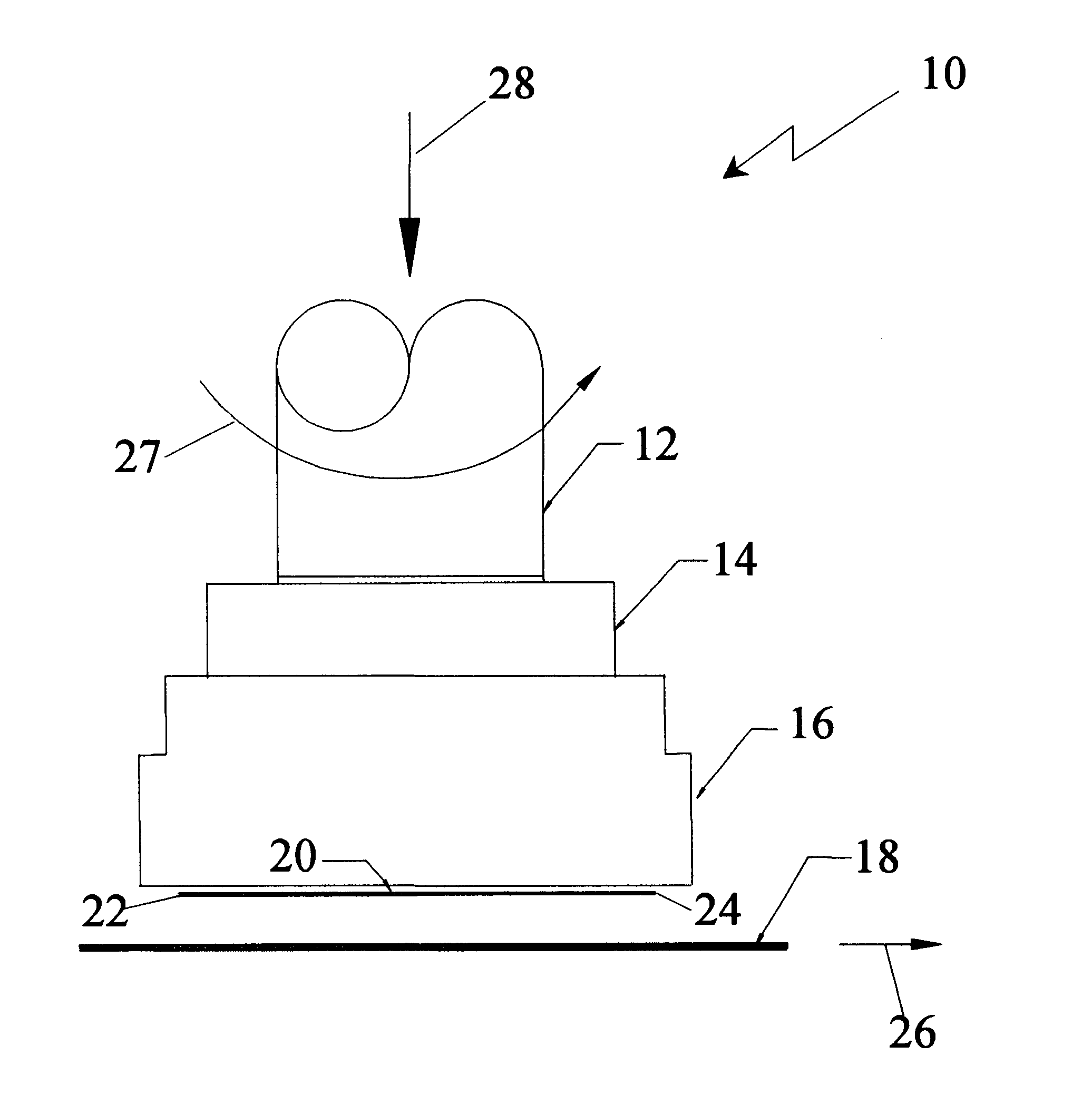
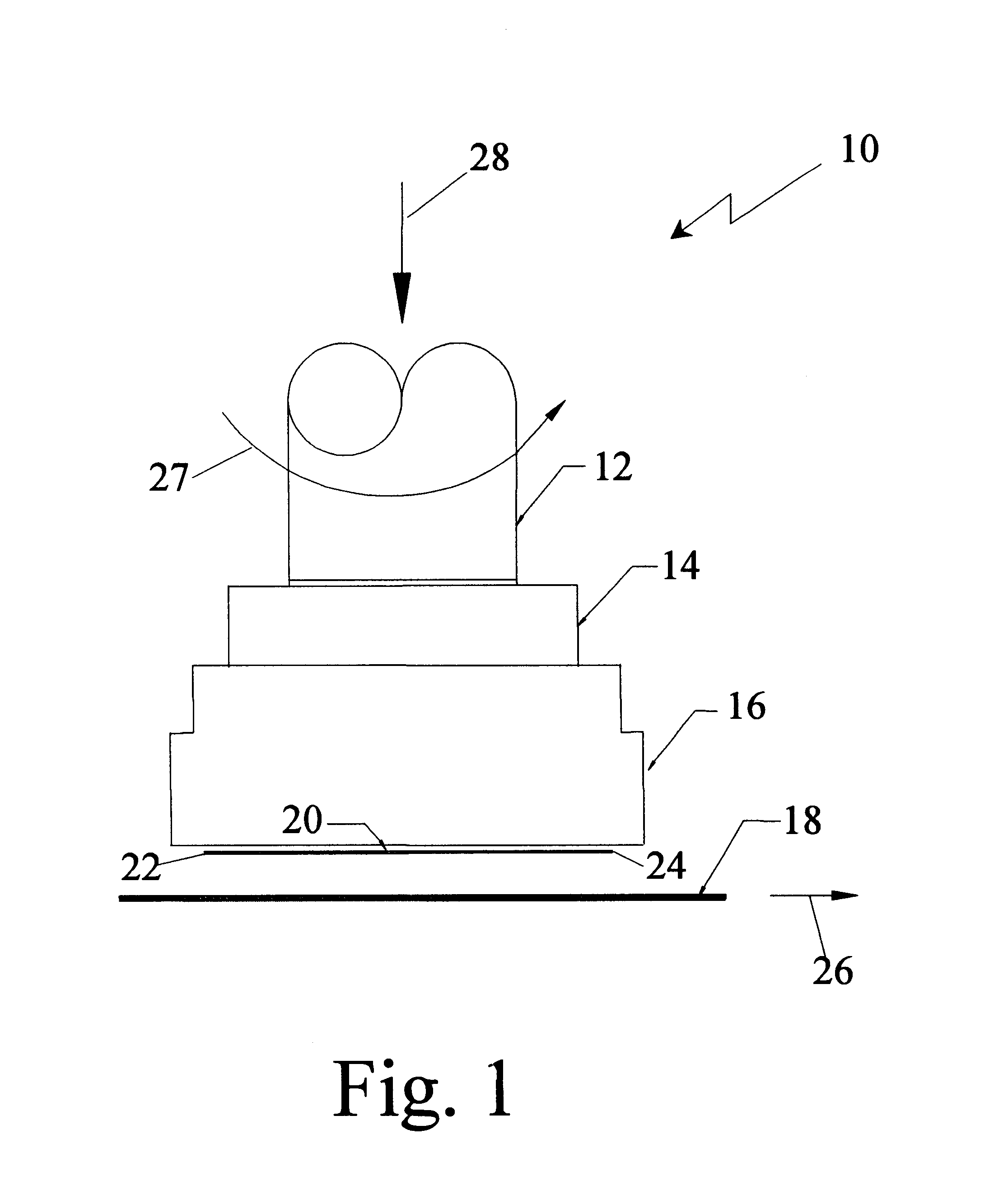
A presently preferred embodiment of a portion of a wafer polishing apparatus 10 is generally illustrated in FIG. 1. One example of a wafer polishing apparatus 10 is part of the TERES.TM. Chemical Mechanical Polishing (CMP) system available from Lam Research Corporation located in Fremont, Calif. FIG. 1 is a front view of the portion of the wafer polishing apparatus 10 that includes a spindle 12, a head exchanger assembly 14, a wafer polishing assembly 16 and a polishing pad 18.

The wafer polishing apparatus 10 is operable to polish and planarize objects that, in the presently preferred embodiment, are a semiconductor wafer 20. Other objects such as, for example, quartz crystals, ceramic elements, lenses, glass plates and other wafer like work pieces may also be planarized and polished by the wafer polishing apparatus 10. The semiconductor wafers 20, hereinafter referred to as wafers 20, are circular shaped discs that are separable into individual chips containing integrated circuits....


PUM

PropertyMeasurementUnit
thickaaaaaaaaaa
distanceaaaaaaaaaa
thicknessaaaaaaaaaa

Abstract

A polishing head assembly for retaining an object that is subject to polishing with a polishing pad is disclosed. The polishing head assembly comprises a head retainer assembly movably coupled to a wafer carrier head. The head retainer assembly includes a gimbal post and a load suspension plate. The gimbal post and the load suspension plate are operable to transfer a loading force to the wafer carrier head during polishing. The gimbal post also provides gimballing to optimize the position of the object in parallel with the polishing pad. In addition, the load suspension plate provides distribution of the loading force to optimize the flatness of the object during polishing.

Description

The present invention relates to planarization of semiconductor wafers using a chemical mechanical planarization technique. More particularly, the present invention relates to a wafer polishing head assembly for use in chemical mechanical polishing / planarization of semiconductor wafers.Semiconductor wafers are typically fabricated with multiple copies of a desired integrated circuit design that will later be separated and made into individual chips. Wafers are commonly constructed in layers, where a portion of a circuit is created on a layer and conductive vias are created to electrically connect the circuit to other layers. After each layer of the circuit is etched on the wafer, an oxide layer is put down allowing the vias to pass through but covering the rest of the previous circuit level. Each layer of the circuit can create or add unevenness to the wafer that is typically smoothed before generating the next circuit layer.Chemical mechanical planarization (CMP) techniques are use...

Claims


Application Information

Patent Timeline
Patent Type & Authority Patents(United States)
IPC IPC(8): B24B37/04B24B37/30
CPCB24B37/30
Inventor PHAM, XUYEN N.
Owner APPLIED MATERIALS INC
Why Eureka
Try Eureka