Programmable compensated delay for DDR SDRAM interface using programmable delay loop for reference calibration

a programmable delay and sdram technology, applied in time-delay networks, instruments, generating/distributing signals, etc., can solve problems such as temperature and voltage, and affect delay

Inactive Publication Date: 2004-07-06
MARVELL ASIA PTE LTD
View PDF6 Cites 74 Cited by
  • Summary
  • Abstract
  • Description
  • Claims
  • Application Information

AI Technical Summary

Problems solved by technology

Temperature and volta

Method used


Image

  • Programmable compensated delay for DDR SDRAM interface using programmable delay loop for reference calibration
  • Programmable compensated delay for DDR SDRAM interface using programmable delay loop for reference calibration
  • Programmable compensated delay for DDR SDRAM interface using programmable delay loop for reference calibration

Examples


Embodiment Construction

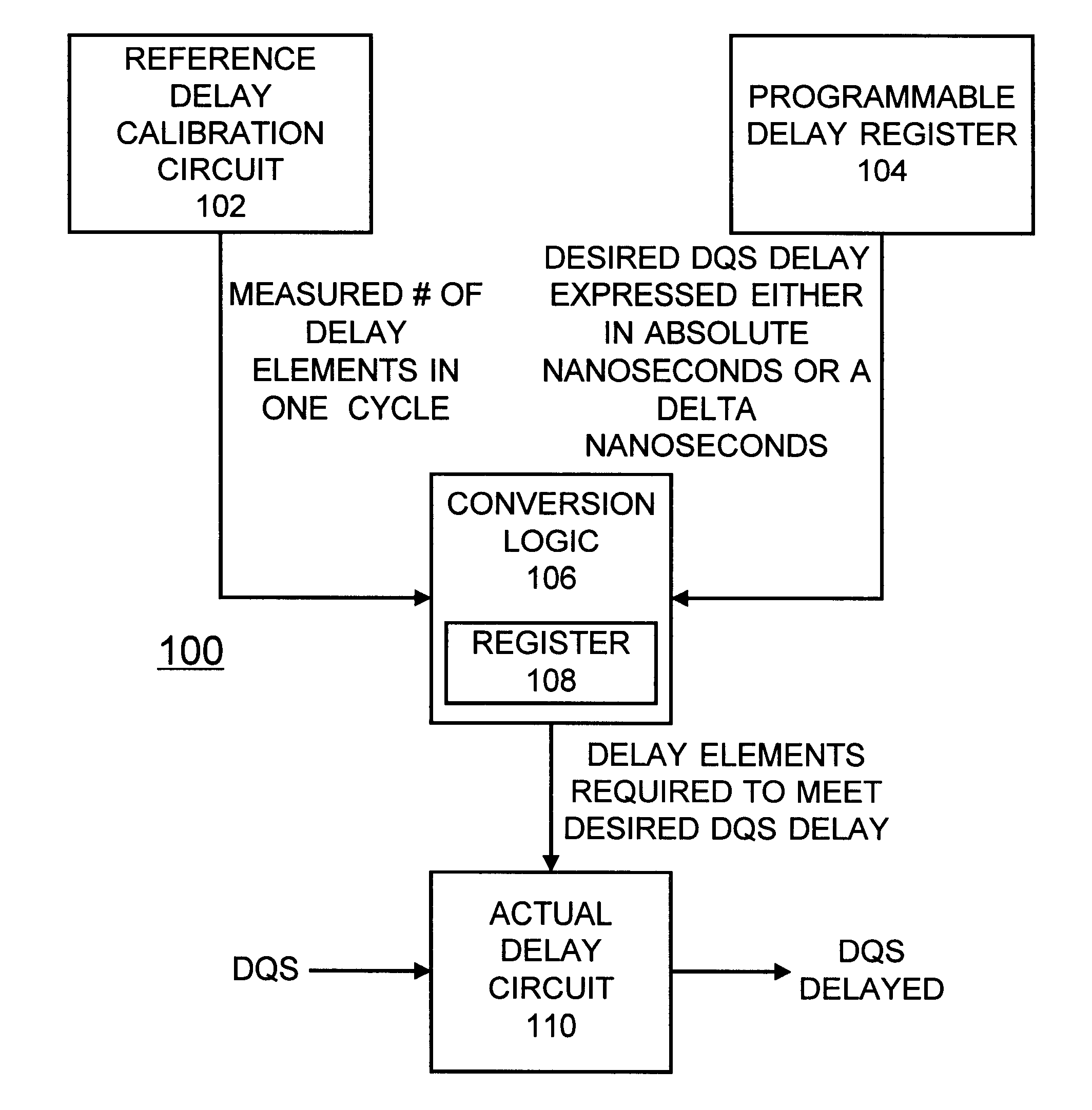
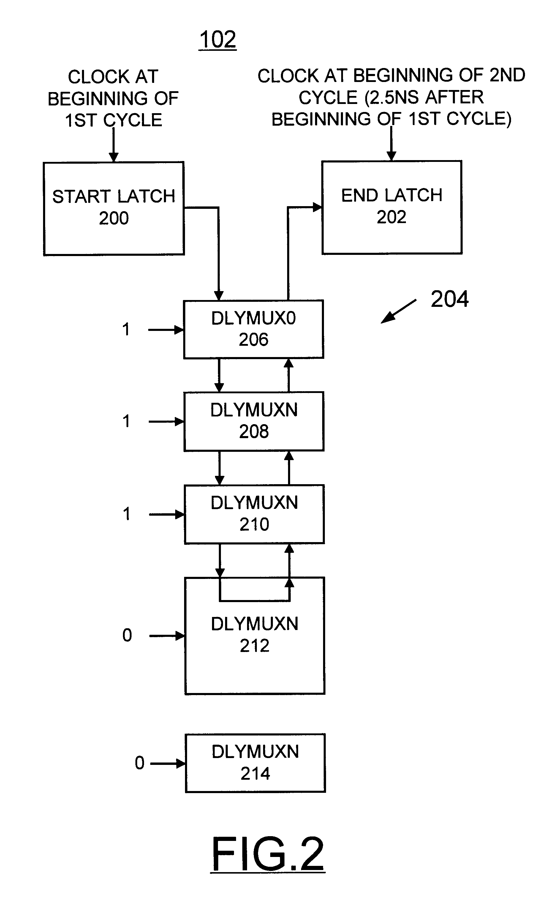
Having reference now to the drawings, in FIG. 1, there is shown a programmable compensated delay apparatus in accordance with the preferred embodiment generally designated by the reference character 100. Programmable compensated delay apparatus 100 includes a reference delay calibration circuit 102, a programmable delay register 104, a conversion logic 106 and an actual delay circuit 110.

In accordance with features of the preferred embodiment, programmable compensated delay apparatus 100 supports programming a desired delay value for DQS form a selectable range of delays. An original delay setting for DQS is obtained from SDRAM read timing analysis using timing run output information on a pre-fabricated design. Programmable compensated delay apparatus 100 provides the capability to program a delay value allowing for adjustments based on measured results for the DQ data and DQS strobe on actual hardware. Programmable compensated delay apparatus 100 is implemented to provide delay com...


PUM


Abstract

A programmable compensated delay for a double data rate (DDR) synchronous dynamic random access memory (SDRAM) interface is provided. A programmable compensated delay apparatus includes a reference delay calibration circuit for providing a measured number of delay elements in one cycle. A programmable delay register provides a desired delay value. A conversion logic is coupled to the reference delay calibration circuit and the programmable delay register for receiving both the measured number of delay elements in one cycle and the desired delay value. The conversion logic provides a number of required delay elements. A delay circuit is coupled to the conversion logic for receiving the number of required delay elements and providing the desired delay. A SDRAM control logic provides a refresh start signal to the reference delay calibration circuit for updating the delay circuit during each DRAM refresh. The DQS clock strobe on the DDR SDRAM is applied to the delay circuit and is delayed by the desired delay.

Description

The present invention relates generally to the data processing field, and more particularly, relates to a programmable compensated delay for a double data rate (DDR) synchronous dynamic random access memory (SDRAM) interface.DESCRIPTION OF THE RELATED ARTDDR SDRAM use a source synchronous interface for reading and writing data. The source synchronous clock strobe on DDR SDRAM is named DQS. When data is read from a DDR SDRAM, the DQS clock strobe is driven by the SDRAM. The SDRAM edge aligns the DQS clock strobe with the data. It is the responsibility of the device receiving SDRAM read data to delay the incoming DQS and center the incoming DQS in the middle of the incoming data. Strobe centering relative to data is required to handle skew uncertainty between the DQS and data coming out of the SDRAM, as determined by the SDRAM specification. It is also required to handle skew uncertainty created by card wiring, card loading, and inter-signal interference (ISIS). Lastly, DQS centering ...

Claims


Application Information

Patent Timeline
IPC IPC(8): G06F13/42
CPCG06F13/4243
Inventor BORKENHAGEN, JOHN MICHAELMARCELLA, JAMES ANTHONY
Owner MARVELL ASIA PTE LTD
Why Eureka
Try Eureka