Electroluminescent devices

a technology of electroluminescent devices and electrodes, applied in the direction of basic electric elements, electrical appliances, instruments, etc., can solve the problems of reducing the service life of the device, limiting the use of the device, and unable to substitute for the ito coated substra

Inactive Publication Date: 2004-08-17
PELIKON
View PDF16 Cites 57 Cited by
  • Summary
  • Abstract
  • Description
  • Claims
  • Application Information

AI Technical Summary

Problems solved by technology

However, the short lifetimes (around 500 hrs) of such devices limited their use.
It is also known to reduce moisture ingression into EL lamps, which would otherwise degrade the ZnS and greatly reduce the service life of the device, by the technique of microencapsulation, where the individual phosphor particles 3 are coated in glass or ITO 4.
Although a range of alternative transparent conductors have been tried (including, transparent conductive polymers and screen printed ITO), at present there appears to be no alternative to the ITO coated substrate.
This transparent conductor must be coated onto a transparent substrate using a proprietary process and this is an expensive part of the device (accounting for up to 50% of the production cost).
Apart from expense, there are other problems relating to the use of a transparent electrode coating:
In order to get fine resolution in a prior art lamp used as a display, areas of the ITO conduction layer must be removed to produce an electrode pattern using either laser oblation or an etching process, further adding to the cost of manufacture.
The need for a transparent substrate and transparent conductor limits the application possibilities.
The ITO is not a good conductor and therefore requires high current densities to enable such a device to function acceptably.
Using two different processes to create the top and bottom electrodes creates registration. difficulties, which become critical when fine resolution devices are manufactured.
LEDs or other lamps are expensive to make.
It is expensive to locate LEDs and other lamps within a plastic moulding.
LEDs do not give high resolution and so limit the size of the characters of an alphanumeric display
LCDs are expensive because they have sensitive production processes that demand a high level of precision and they require glass substrates.
This expense means that the production of such displays is only commercially viable at mass production volumes.

Method used


Image

  • Electroluminescent devices
  • Electroluminescent devices
  • Electroluminescent devices

Examples


first embodiment

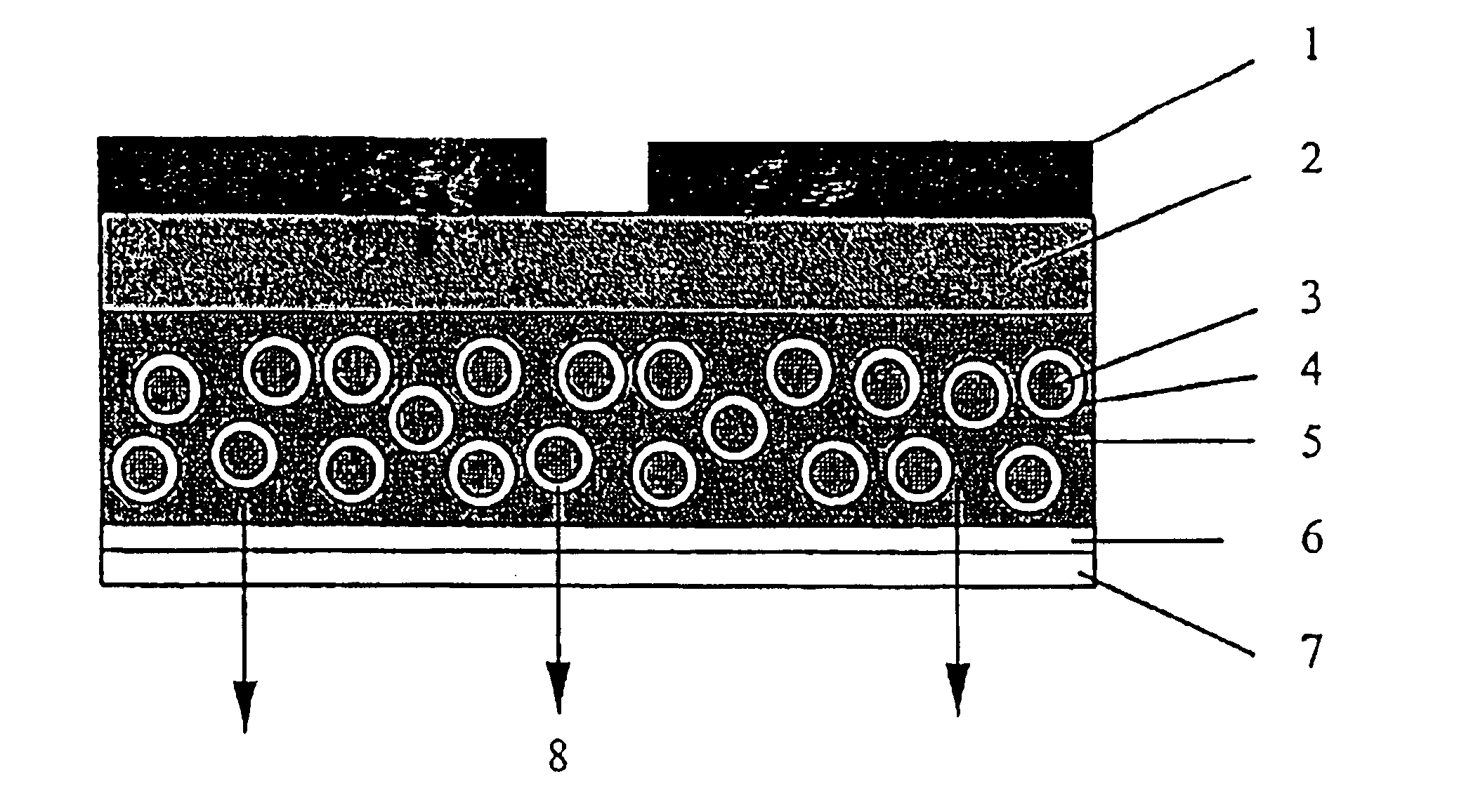
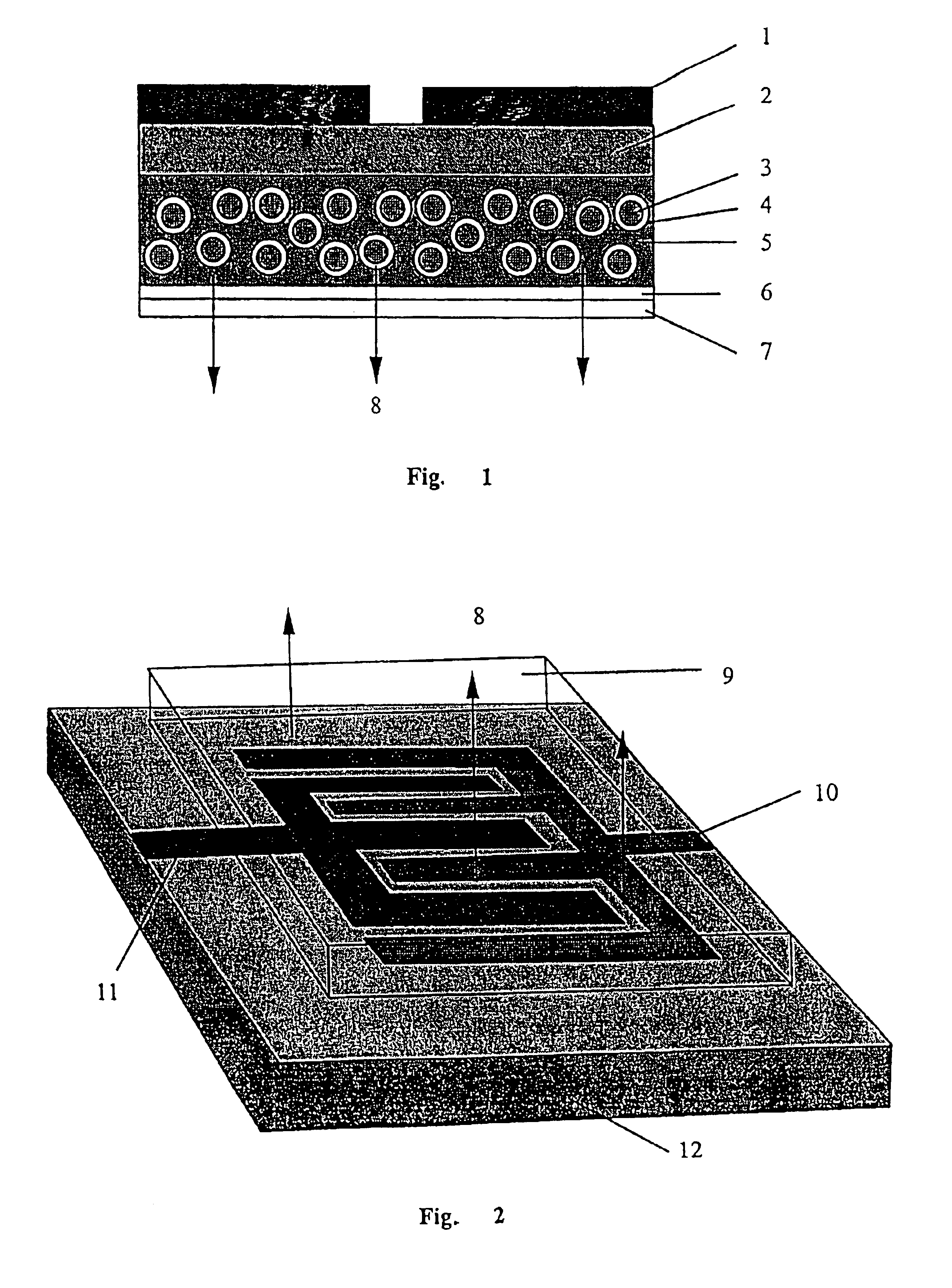
In the invention, instead of creating the electric field between two planar electrodes as in the prior art (see FIG. 1), the electric field is generated laterally across a single plane between adjacent electrodes applied to a base substrate (see FIG. 2). These adjacent electrodes may, for instance, be interdigitated as shown in FIG. 2 or they may be formed in another shape, as determined by the particular application.

FIG. 2 shows an electroluminescent illuminating means according to a first embodiment of the invention. An electroluminescent substance 9 such as a phosphor (powder film) layer or a phosphor (powder film) layer together with a dielectric sandwich layer lies above a pattern of two electrodes 10, 11 which are interdigitated and which, in turn, lie on a base substrate 12. When appropriate electric signals are applied to the two electrodes 10, 11, the electroluminescent substance emits light 8.

An electroluminescent illuminating means according to the first embodiment of the...

second embodiment

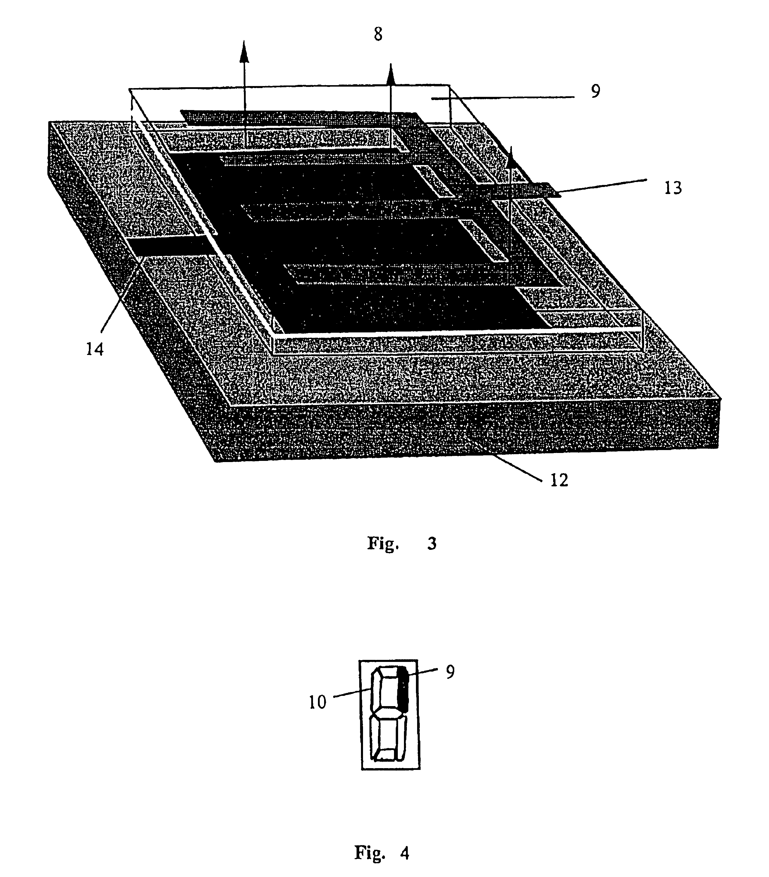
In the invention, instead of creating the electric field between two full area planar electrodes (see FIG. 1) and allowing the light to escape through the transparent top electrode 6 the field is generated between two planar electrodes which are formed so as to allow light to escape through gaps created in one (or both) of the electrodes (see FIG. 3).

FIG. 3 shows an electroluminescent illuminating means according to a second embodiment of the invention. An electroluminescent substance 9 such as a phosphor (powder film) layer or a phosphor (powder film) layer together with a dielectric sandwich layer lies above a first electrode 14 which lies on a base substrate 12. A second electrode 13 is formed on top of the electroluminescent substance. The second electrode 13 does not fully cover the electroluminescent substance 9 and when appropriate-electric signals are applied to the two electrodes, the electroluminescent substance 9 emits light 8 `around` the second electrode 13.

An electrolu...


PUM


Abstract

An electroluminescent lamp or display comprises a first electrode on a substrate interdigitated with a second electrode on the same substrate. A layer of electroluminescent material is provided over the electrodes. The arrangement has the advantage that light from the electroluminescent material does not need to pass through either of the electrodes. The substrate may be a printed circuit board. In an alternative embodiment the second electrode is provided over the layer of electroluminescent material and gaps are provided in the electrode for the emission for light. The electroluminescent lamps may be used to form a seven-segment display.

Description

This is the U.S. national phase of International Application No. PCT / GB99 / 01233 filed Apr. 22, 1999.1. Field of the InventionThe present invention relates to electroluminescent (EL) devices, in particular to electroluminescent displays.2. Background ArtElectroluminescence is the emission of light from a substance under electric-field excitation.Phosphor electroluminescence was discovered and documented in 1936, but it was not until the 1950's that GTE Sylvania received a patent for an EL powder lamp. However, the short lifetimes (around 500 hrs) of such devices limited their use. Work carried out in the 1980's revitalised the powder EL lamp and in 1990 the Durel Corporation demonstrated a flexible EL phosphor device that was incorporated into a LCD flat panel display as a backlight. The manufacturing technique involved encapsulating the phosphor powder particles in glass beads and sandwiching the powder, which is held in a dielectric matrix, between two electrodes. An AC voltage was...

Claims


Application Information

Patent Timeline
Patent Type & Authority Patents(United States)
IPC IPC(8): H05B33/26H05B33/10H05B33/12H05B33/14H01L21/02H01L21/203H01L31/00H05B33/22H05B41/16
CPCH05B33/10H05B33/12H05B33/26
Inventor BARNARDO, CHRISTOPHER J. A.FRYER, CHRISTOPHER J. N.DAVIES, CHRISTOPHERCOX, PAUL
Owner PELIKON
Why Eureka
Try Eureka