Heterojunction bipolar transistor having wide bandgap material in collector

a bipolar transistor and collector technology, applied in the field of heterojunction bipolar transistors, can solve the problems of catastrophic failure of devices, increased collector doping, and reduced collector doping, so as to improve the medium and high current breakdown voltage, and the effect of reducing the collector doping

Inactive Publication Date: 2004-10-19
WJ COMM
View PDF2 Cites 18 Cited by
  • Summary
  • Abstract
  • Description
  • Claims
  • Application Information

AI Technical Summary

Benefits of technology

The standard heterojunction bipolar transistor has a uniformly doped collector which is normal for providing a high breakdown voltage. In accordance with the invention, a layer of wider bandgap (e.g., the separation between the energy of the lowest conduction band and that of the highest valence band) material i...

Problems solved by technology

If one attempts to operate a HBT beyond the SOA boundaries in the non-safe operating areas as shown in the figure, the device will catastrophically fail.
Fu...

Method used


Image

  • Heterojunction bipolar transistor having wide bandgap material in collector
  • Heterojunction bipolar transistor having wide bandgap material in collector
  • Heterojunction bipolar transistor having wide bandgap material in collector

Examples


Embodiment Construction

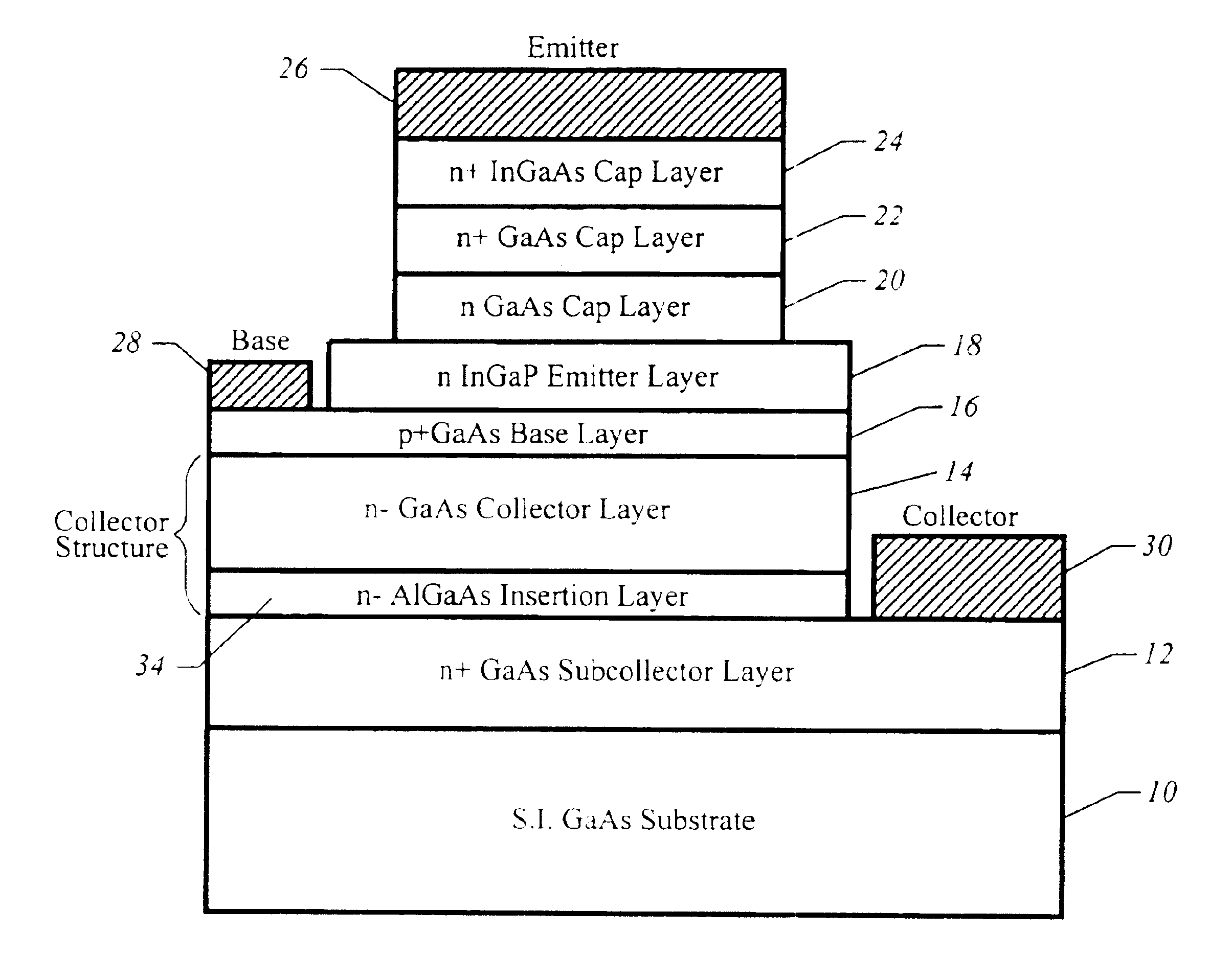
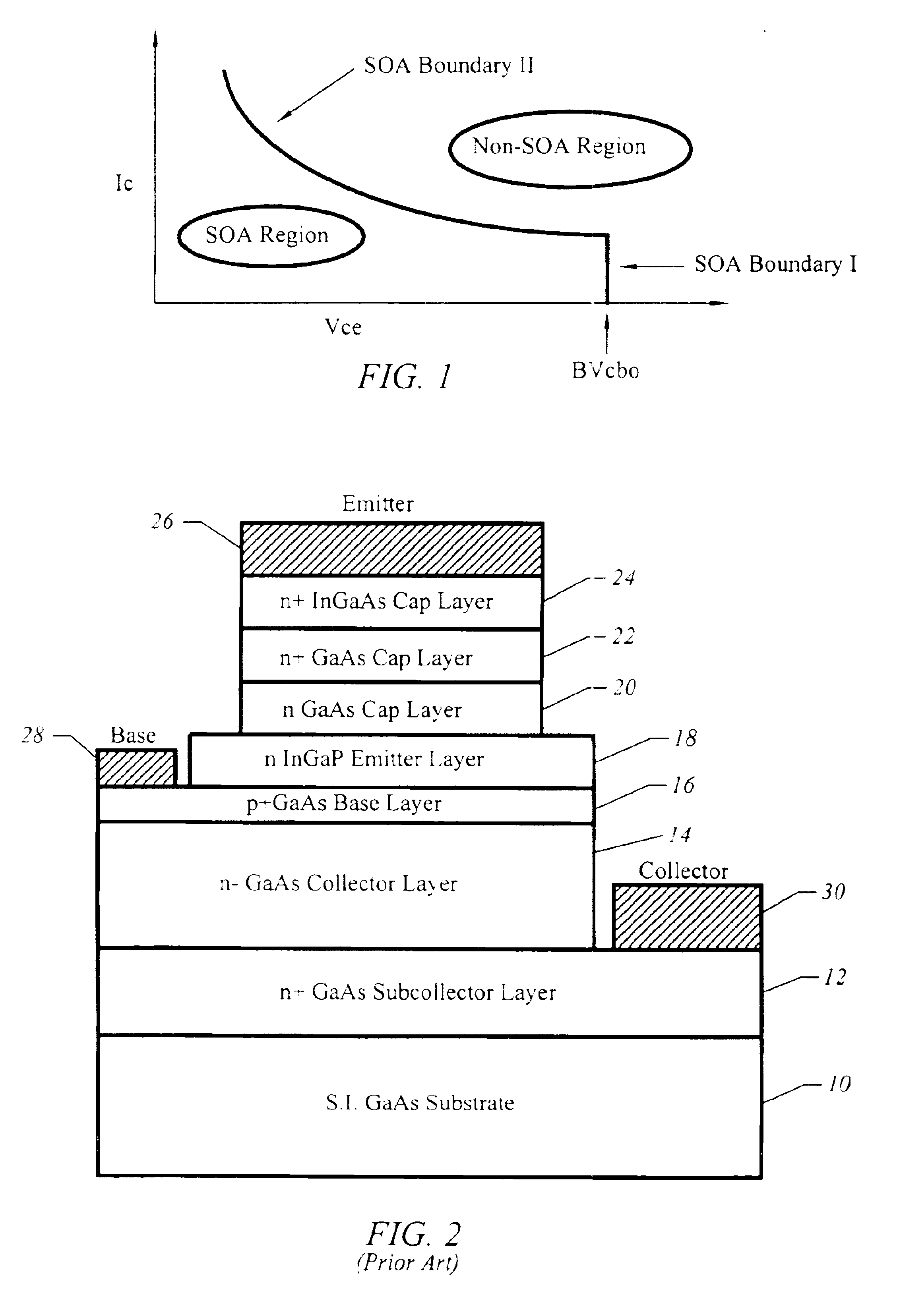
FIG. 2 is a section view of a conventional heterojunction bipolar transistor which includes a GaAs substrate 10 on which is formed an N.sup.+ GaAs subcollector layer 12 with an N.sup.- GaAs collector layer 14 on the subcollector layer. The base layer comprises a P.sup.+ GaAs layer 16 and the emitter includes an N InGaP layer 18. Formed on emitter layer 18 is an N GaAs cap layer 20 with an N.sup.+ GaAs cap layer 22 and an N.sup.+ InGaAs cap layer 24 overlying emitter layer 18. Contacts 26, 28, and 30 are provided to the emitter, base, and collector, respectively.

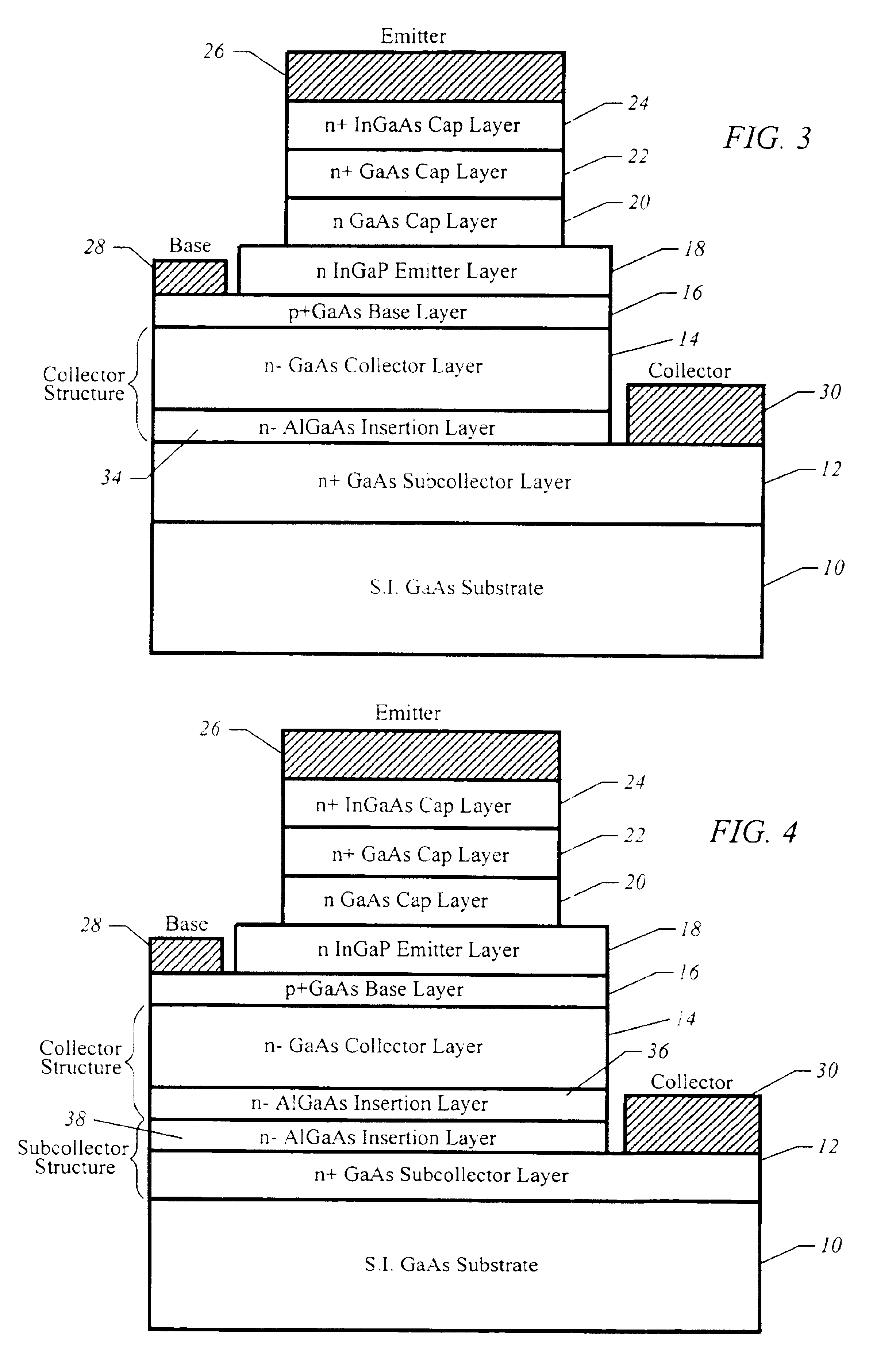
Since the Kirk effect induced breakdown occurs near the collector-subcollector junction, in accordance with the invention a layer of wider bandgap material is inserted at the collector-subcollector junction to thereby increase the breakdown voltage and move the SOA Boundary II upward as shown in FIG. 1 to higher currents. Using the same reference numerals for common elements in FIGS. 2 and 3, FIG. 3 illustrates one embodiment...


PUM


Abstract

The safe operating area (SOA) in a heterojunction bipolar transistor is improved by inserting a material between the collector and subcollector of the transistor with the insertion layer being a material having a wider energy bandgap than the material of the collector. The insertion layer increases the breakdown field at the collector-subcollector junction and thereby increases the Kirk effect induced breakdown voltage.

Description

BACKGROUND OF THE INVENTIONThis invention relates generally to heterojunction bipolar transistors (HBT), and more particularly the invention relates to improving the safe-operating area (SOA) of such a transistor.Heterojunction bipolar transistors (e.g. III-V compound semiconductor) are used in amplifier circuits for telecommunications applications. A major concern lies in operating the transistors in safe-operating areas (SOA) to prevent overdrive and failure of the devices. As shown in FIG. 1, the SOA is defined by two boundaries. The first boundary, SOA Boundary I, is limited by the open-emitter base-collector junction breakdown voltage, BVcbo, of the transistor. This boundary sets the operating limit of the transistor at low current densities. The second boundary, SOA Boundary II, is related to the collector breakdown when substantial injected current carriers are present in the collector. This boundary is important at medium to high current levels. If one attempts to operate a ...

Claims


Application Information

Patent Timeline
IPC IPC(8): H01L29/66H01L31/0264H01L29/737H01L31/0328H01L29/08
CPCH01L29/7371H01L29/0821
Inventor CHAU, HIN FAIDUNNROWICZ, CLARENCE JOHNCHEN, YANLEE, CHIEN PING
Owner WJ COMM
Why Eureka
Try Eureka