Flash memory having local SONOS structure using notched gate and manufacturing method thereof

a technology of flash memory and sonos structure, which is applied in the direction of semiconductor devices, electrical devices, transistors, etc., can solve the problems of significant overlap variation, difficulty in combining (or integrating) on one chip, and inability to completely perform erase operations

Inactive Publication Date: 2004-10-19
SAMSUNG ELECTRONICS CO LTD
View PDF17 Cites 48 Cited by
  • Summary
  • Abstract
  • Description
  • Claims
  • Application Information

AI Technical Summary

Problems solved by technology

Because of the high threshold voltage Vth, it is difficult to merge (or integrate) on one chip both the stacked SONOS-type cell and general logic product having a low initial threshold voltage Vth.
In addition, in the stacked SONOS-type cell 10, electrons trapped in the nitride layer 2 can move laterally along the nitride layer, and thus an erase operation may not be completely performed.
During the photography portion of the photolithography process, misalignment can occur, resulting in significant overlap variation.

Method used


Image

  • Flash memory having local SONOS structure using notched gate and manufacturing method thereof
  • Flash memory having local SONOS structure using notched gate and manufacturing method thereof
  • Flash memory having local SONOS structure using notched gate and manufacturing method thereof

Examples


Embodiment Construction

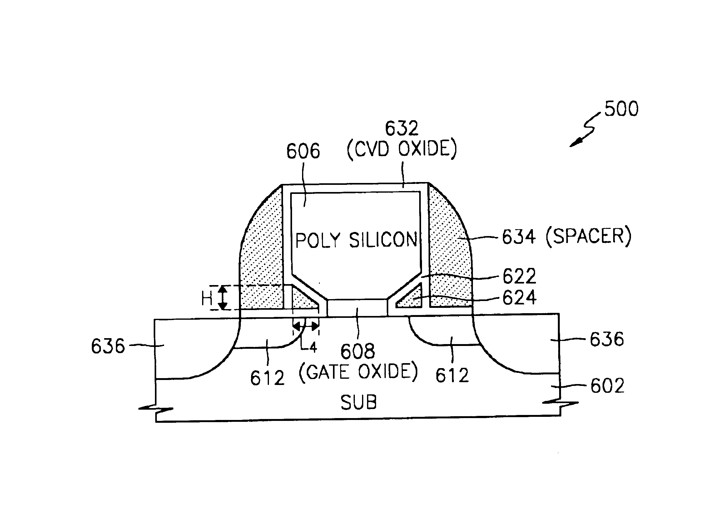
An embodiment of the present invention provides a local SONOS-type structure, e.g., a cell for nonvolatile semiconductor memory, which can solve the above and other problems of the local SONOS-type cells according to the Background Art. This embodiment can exhibit (1) a reduced initial threshold voltage Vth and / or (2) an increased number of programming operations and erase operations for which a predetermined data retention time can be maintained, relative to the Background Art.

An embodiment of the invention provides a method of forming a local SONOS-type structure having a notched gate electrode.

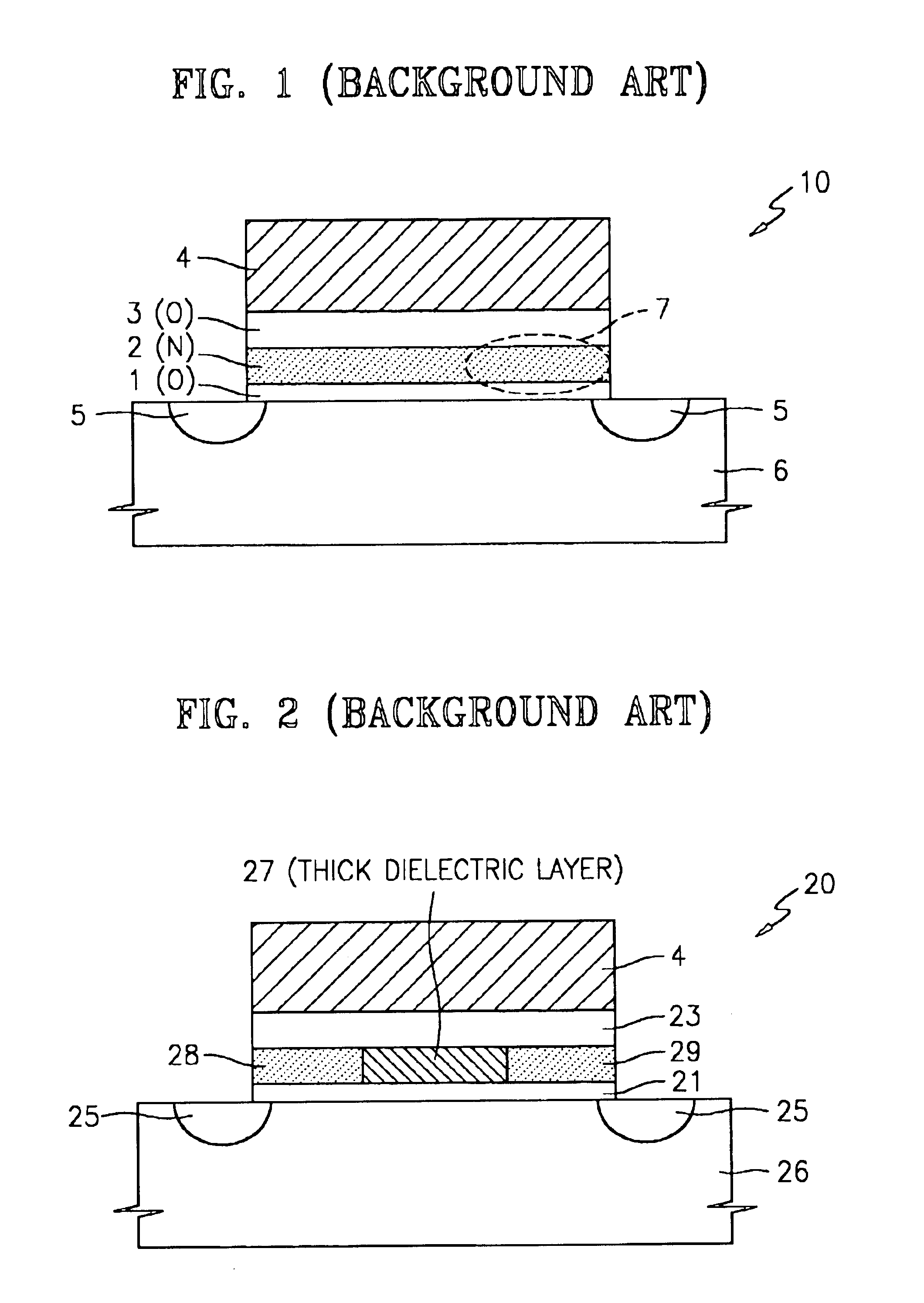
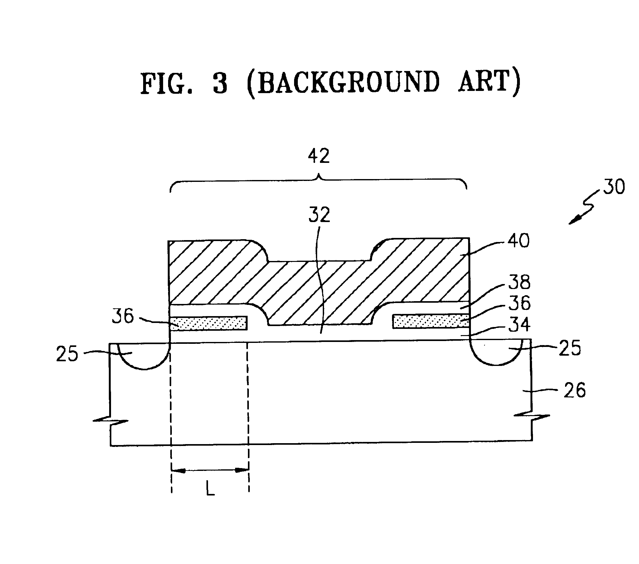
An embodiment of the invention represents the recognition of a flaw in a rationale according to the Background Art, the rationale being: the preferred technique for forming SONOS-type structures is to successively deposit oxide, nitride, oxide and polysilicon layers and then pattern the layers to form a gate electrode having underlying ONO structures via photolithography despite the tendenc...


PUM


Abstract

A notched gate SONOS transistor includes: a substrate having source / drain regions; a gate insulator layer on the substrate between the source / drain regions; a notched gate structure, on the gate insulator leyer, having at least one notch; and at least one ONO wedge structure in the at least one notch, respectively, of the gate structure.

Description

DESCRIPTION OF THE BACKGROUND ARTIn general, semiconductor memory devices for storing data are divided into volatile memory devices, which are likely to lose their data when the power supply is interrupted, and nonvolatile memory devices, which can retain their data even when the power supply is interrupted. Compared to other nonvolatile memory technologies, e.g., disk drives, nonvolatile semiconductor memories are relatively small. Accordingly, nonvolatile memory devices have been widely employed in mobile telecommunications systems, memory cards, etc.Recently, nonvolatile memory devices having silicon-oxide-nitride-oxide-silicon (SONOS) structures, e.g., SONOS-type nonvolatile memory devices, have been proposed. The SONOS-type nonvolatile memory devices have thin cells which are simple to manufacture and can be easily incorporated, e.g., into a peripheral region and / or a logic region of an integrated circuit.A SONOS-type nonvolatile semiconductor memory device according to the Bac...

Claims


Application Information

Patent Timeline
Patent Type & Authority Patents(United States)
IPC IPC(8): H01L21/02H01L21/336H01L21/28H01L29/423H01L29/40H01L29/66H01L29/792H01L21/8247H01L27/115H01L29/788
CPCH01L21/28114H01L21/28273H01L29/7923H01L29/4232H01L29/66833H01L21/28282H01L29/40114H01L29/40117H10B69/00
Inventor KIM, SANG SULEE, NAE-INBAE, GEUM-JONGKIM, KI CHULRHEE, HWA SUNG
Owner SAMSUNG ELECTRONICS CO LTD
Why Eureka
Try Eureka