Mobile communication apparatus including dividers in transmitter and receiver

a communication apparatus and divider technology, applied in the field of transmission devices, can solve the problems of difficult to anticipate the dc offset voltage, difficult for a single vco to cover, and the drawback of the direct conversion receiver is a dc offset voltag

Inactive Publication Date: 2004-11-30
TTPCOM
View PDF14 Cites 49 Cited by
  • Summary
  • Abstract
  • Description
  • Claims
  • Application Information

AI Technical Summary

Problems solved by technology

However, since it is difficult for a single VCO to cover these frequency bands, two VCOs are required.
A widely known drawback of the direct conversion receiver is a DC offset voltage.
Therefore, in a system such as GSM, DCS1800, in which a received frequency is not fixed during a call but the frequency hops within a reception band, it is difficult to previously anticipate the DC offset voltage.
The scheme employed in the example of FIG. 11 is not suitable for high speed data communications since a filter intervening in a feedback loop for offset cancellation make the fast offset cancellation difficult.

Method used


Image

  • Mobile communication apparatus including dividers in transmitter and receiver
  • Mobile communication apparatus including dividers in transmitter and receiver
  • Mobile communication apparatus including dividers in transmitter and receiver

Examples


first embodiment

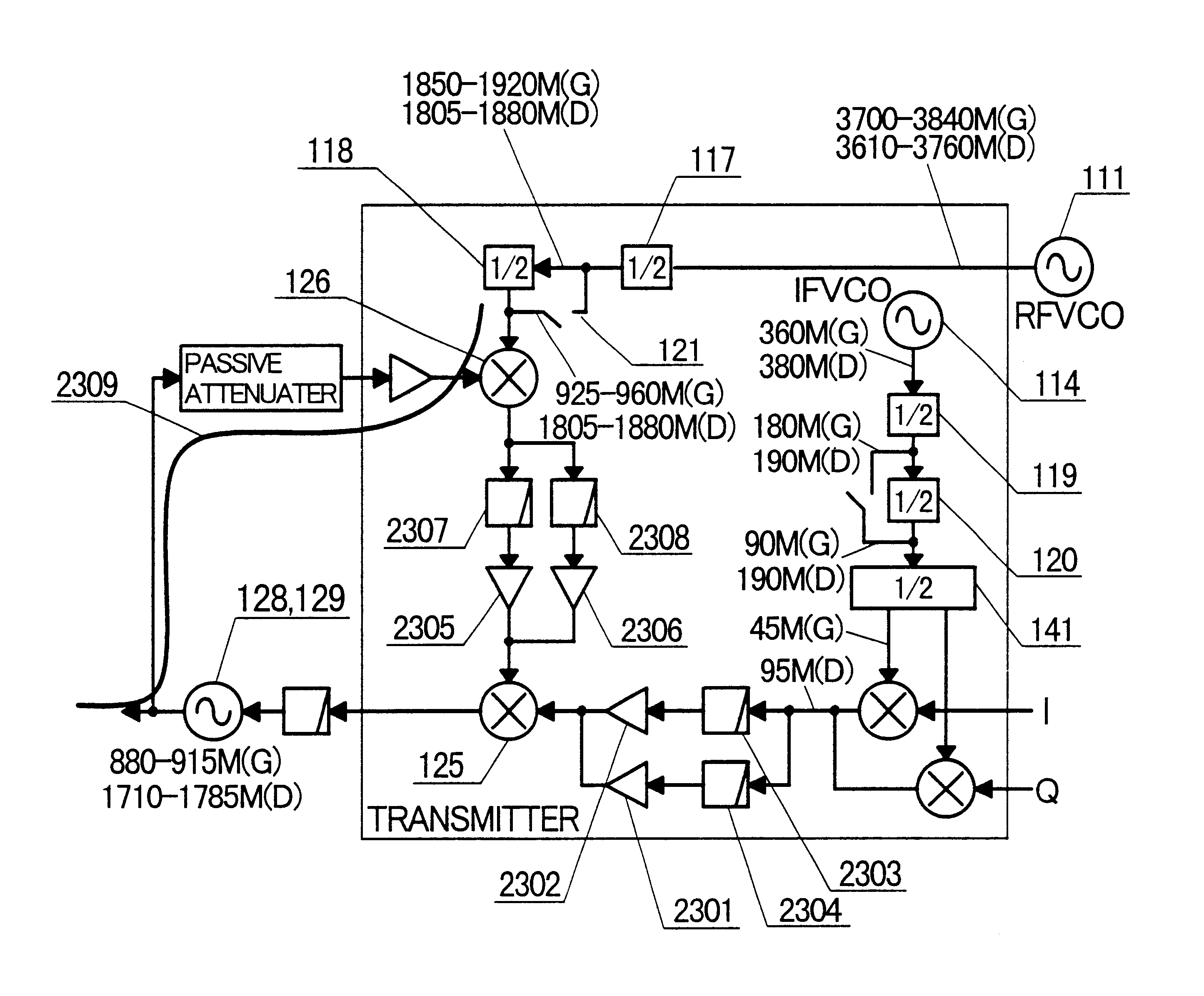
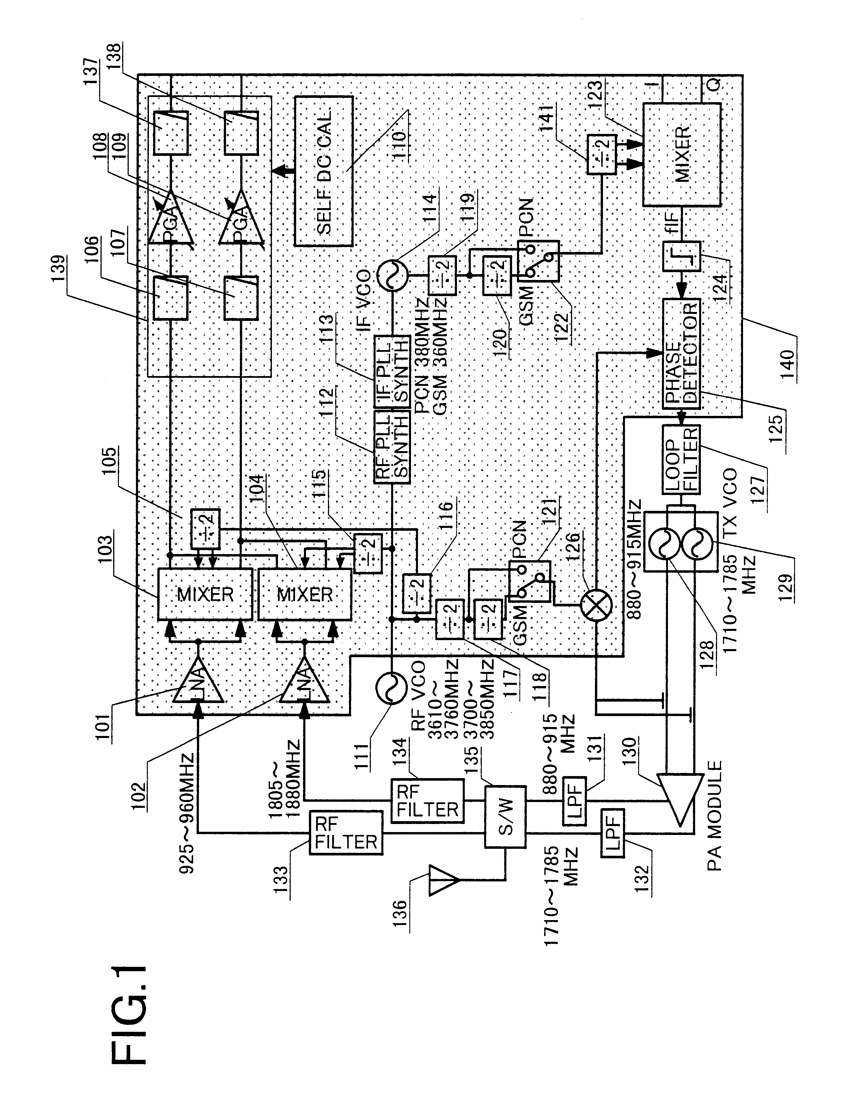
the present invention will be described with reference to FIG. 1. The first embodiment uses an exemplary mobile communication apparatus, as an application, which supports the European cellular telephone GSM (900 MHz band) and DCS1800 (1800 MHz band).

A direct conversion scheme is applied to a receiver for converting an RF signal directly to a baseband signal, and the offset PLL scheme, previously shown in the prior art example, is applied to a transmitter. The receiver comprises low noise amplifiers 101, 102; mixers 103, 104; and a variable gain low pass filter 139. Each of the mixers converts a signal frequency band from the RF band to the baseband, and simultaneously performs demodulation for separating an RF signal into a sine component and a cosine component. For this purpose, the mixers 103, 104 must be applied with locally oscillated signals which are shifted in phase by 90.degree.. The locally oscillated signals are generated using dividers 105, 115. The locally oscillated sig...

second embodiment

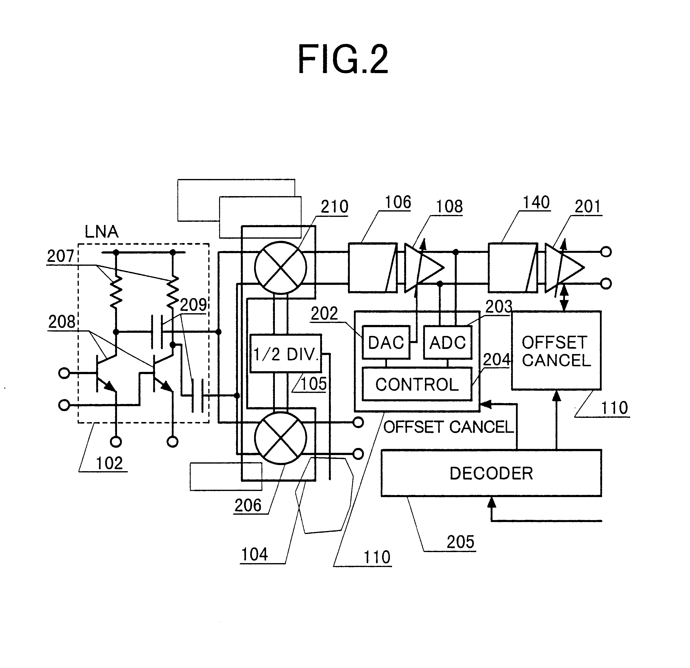
Next, a receiver according to the present invention will be described with reference to FIG. 2.

The illustrated receiver comprises a low noise amplifier 102; a mixer 104; a divider 105; low pass filters 106, 137; variable gain amplifiers 108, 201; DC offset voltage canceling circuits 110; and a decoder 205. The low noise amplifier 102 in turn comprises a load resistor 207; a transistor 208; and a capacitance 209, while the DC offset voltage canceling circuit 110 comprises a digital-to-analog converter (DAC) 202; an analog-to-digital converter (ADC) 203; and a controller 204. The mixer 104 comprises mixers 210, 206.

An output DC voltage of the variable gain amplifier 108 is converted to a digital signal by the ADC 203, and inputted to the controller 204. The controller 204 measures the DC offset voltage at the output of the variable gain amplifier 108 to output a cancel signal for canceling the DC offset voltage. The cancel signal is converted from a digital signal to an analog signal ...

third embodiment

Next, a variable gain amplifier and a DC offset voltage canceling circuit according to the present invention will be described with reference to FIG. 3.

The variable gain amplifier comprises resistors 307, 308, 312; and transistors 309, 310, 311. The transistors 309, 310 are applied with an input voltage at their bases to deliver output voltages from their collectors. The gain can be controlled, for example, by a base voltage of the transistor 311. A DAC 313 comprises transistors 301, 302, 303; and resistors 304, 305, 306. Since the output of a controller 204 is connected to bases of the transistors 301, 302, 303, the controller 204 can control collector DC currents of the transistors 301, 302, 303. The collector DC currents are summed with a collector current of the transistor 309, and then converted to a voltage by the resistor 307. Assume now that a DC offset voltage .DELTA.V (=V.sub.2 -V.sub.1) exists, and the resistance of the resistors 307, 308 are represented by R.sub.L ; an o...


PUM


Abstract

A transceiver suitable for larger scale of integration employs direct conversion reception for reducing the number of filters. Also, the number of VCOs is reduced by utilizing dividers to supply a receiver and a transmitter with locally oscillated signals at an RF band. Dividers each having a fixed division ratio are used for generating locally oscillated signals for the receiver, while a divider having a switchable division ratio are used for generating the locally oscillated signal for the transmitter. In addition, a variable gain amplifier for baseband signal is provided with a DC offset voltage detector and a DC offset canceling circuit for supporting high speed data communications to accomplish fast cancellation of a DC offset by eliminating intervention of a filter within a feedback loop for offset cancellation.

Description

1. Field of the InventionThe present invention relates generally to a mobile communication apparatus which can be implemented with a less number of components, and more particularly, to a transceiver which employs a direct conversion scheme suitable for larger scale of integration.2. Description of the Related ArtWith explosive popularization of mobile communication apparatus, requirements for a reduction in size and cost have been increased. For this reason, it is desired to eliminate VCO (voltage controlled oscillator), reduce the number of filters, and apply integrated circuits with a higher degree of integration. A prior art example of a transceiver which meets such requirements is described in K. Takikawa et. al., "RF Circuits Technique of Dual-Band Transceiver IC for GSM and DCS1800 applications," IEEE 25th European Solid-State Circuits Conference Preprints pp. 278-281, 1999. The configuration of this transceiver is illustrated in FIG. 10A. The illustrated transceiver comprise...

Claims


Application Information

Patent Timeline
Patent Type & Authority Patents(United States)
IPC IPC(8): H04B1/40H04B1/30H04M1/00H04Q7/32H04B1/38H04B1/3822H04B7/00H04L27/38H04M
CPCH04B1/30H03K21/16H03D2200/0047H04B1/40
Inventor TANAKA, SATOSHIWATANABE, KAZUOHOTTA, MASAOHONGO, TOYOHIKOYAMAWAKI, TAIZOKASAHARA, MASUMITAKIKAWA, KUMIKO
Owner TTPCOM
Why Eureka
Try Eureka