Method of manufacturing a wafer

a manufacturing method and technology of a wafer, applied in the direction of basic electric elements, electrical equipment, semiconductor devices, etc., can solve the problems of weakening the pre-determined detachment area, unable to meet the requirements of quality, and the method has a lot of low efficiency

Active Publication Date: 2005-01-04
S O I TEC SILICON ON INSULATOR THECHNOLOGIES
View PDF23 Cites 17 Cited by
  • Summary
  • Abstract
  • Description
  • Claims
  • Application Information

AI Technical Summary

Benefits of technology

The present invention now provides a method of manufacturing a wafer which comprises annealing a heterogeneous material compound that includes a donor substrate of a first material and having a thin layer extending from one face to a weakened zone, with the thin layer bonded to a receiver substrate of a second material that is different from the first material, the annealing being conducted at a temperature and for a time less than that sufficient to cause detachment of the thin layer from the donor substrate, and then irradiating the annealed heterogeneous material compound with photons to obtain detachment of the thin layer from the donor substrate along the weakened zone. Advantageously, the first material has a different coefficient of thermal expansion than that of the second material.

Problems solved by technology

These methods mostly have a very low efficiency due to a lot of process steps and the resulting structures often cannot be produced with the required quality.
This annealing step directly after the implanting step results in a weakening of the pre-determined detachment area 95 due to formation and growth of micro-cracks in the implanted region.
Therefore, the weakening effect resulting from this annealing step is relatively minor.
This method results in disadvantageous boron doping of the surrounding layers and is, especially due to the additional implantation step, expensive and time-consuming.
However, this high dose ion implantation raises the cost of manufacture.
This method causes an additional process step and results in a significant material consumption because the removed material is lost.

Method used


Image

  • Method of manufacturing a wafer
  • Method of manufacturing a wafer
  • Method of manufacturing a wafer

Examples


Embodiment Construction

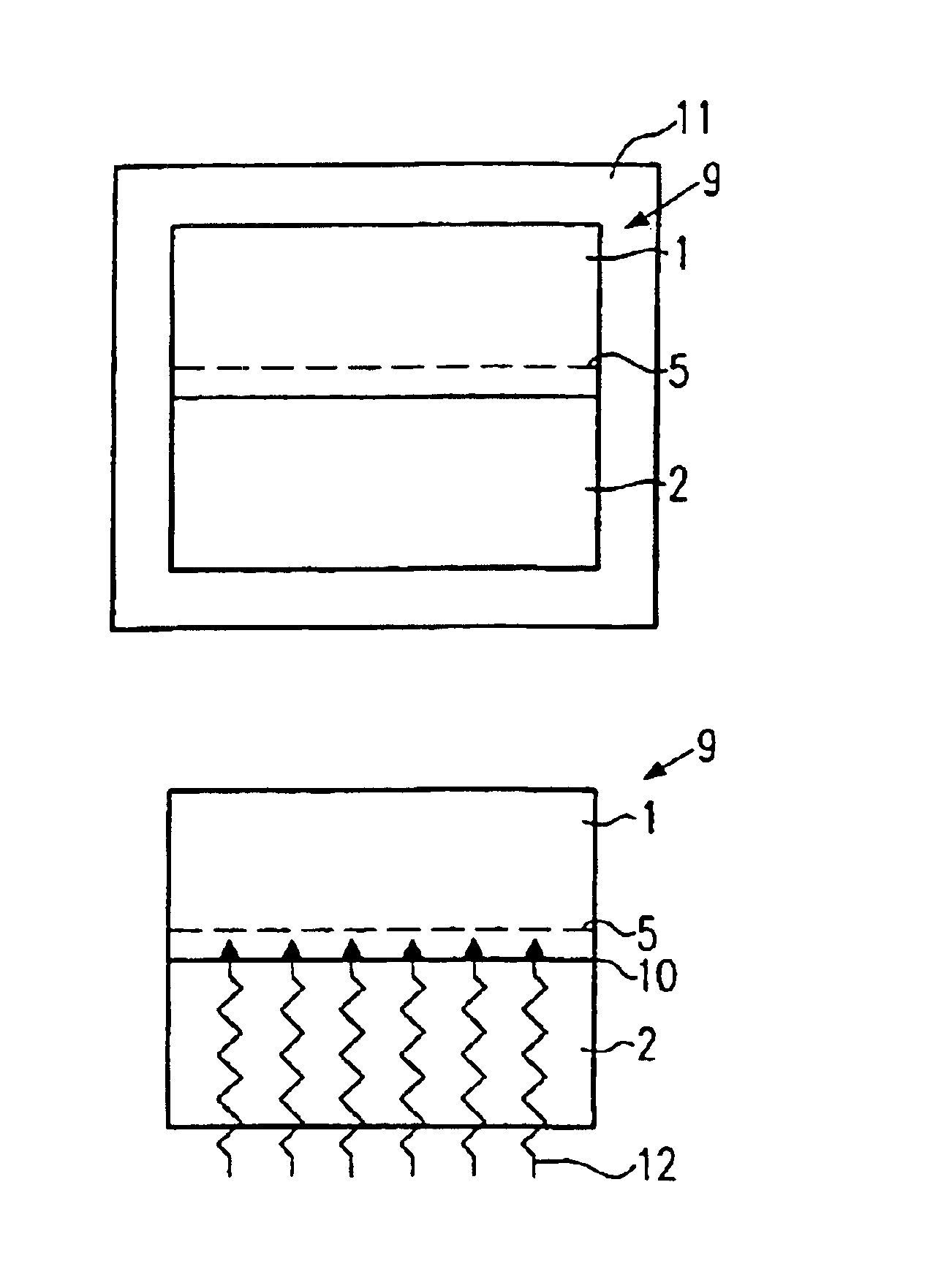
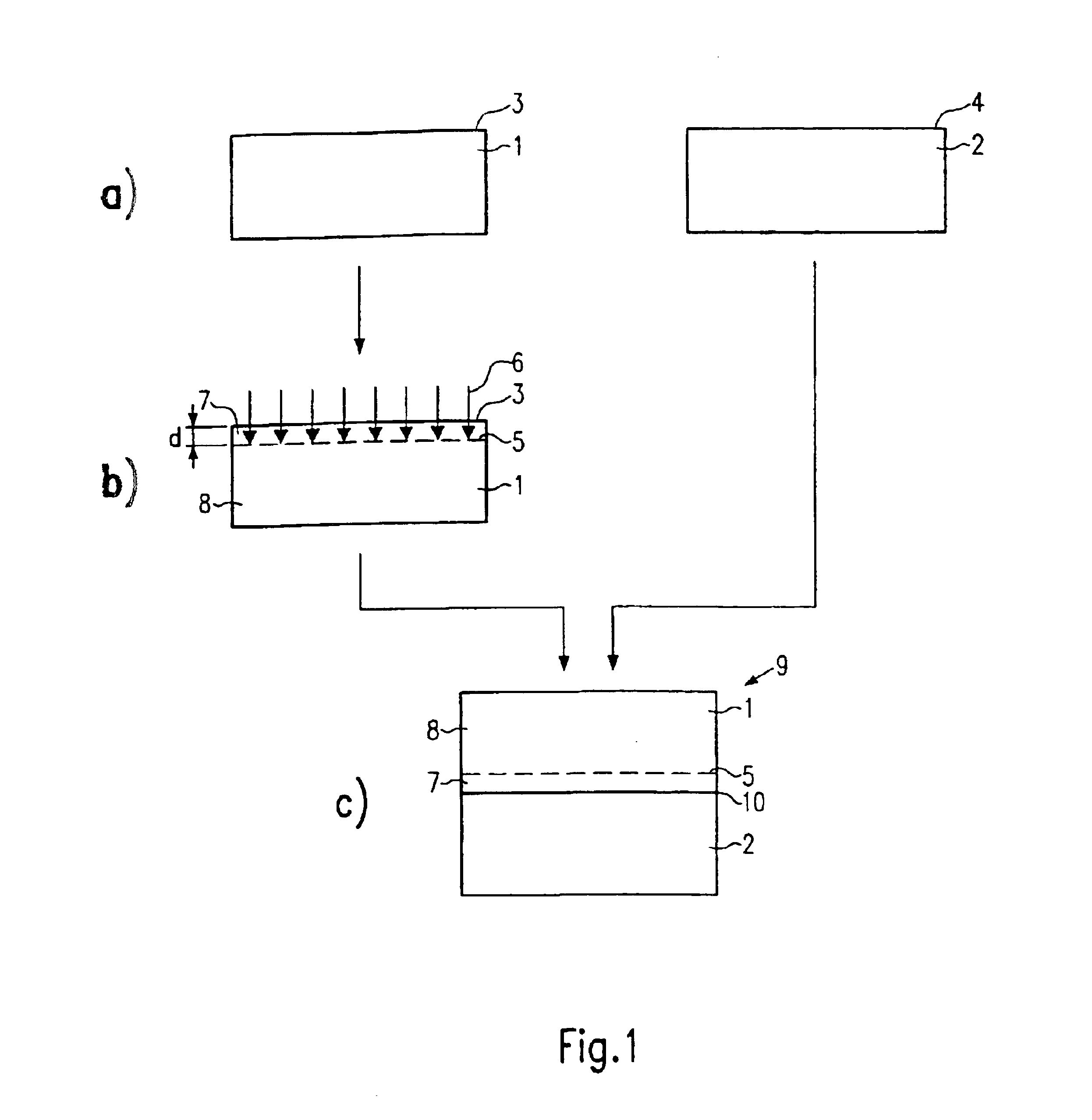
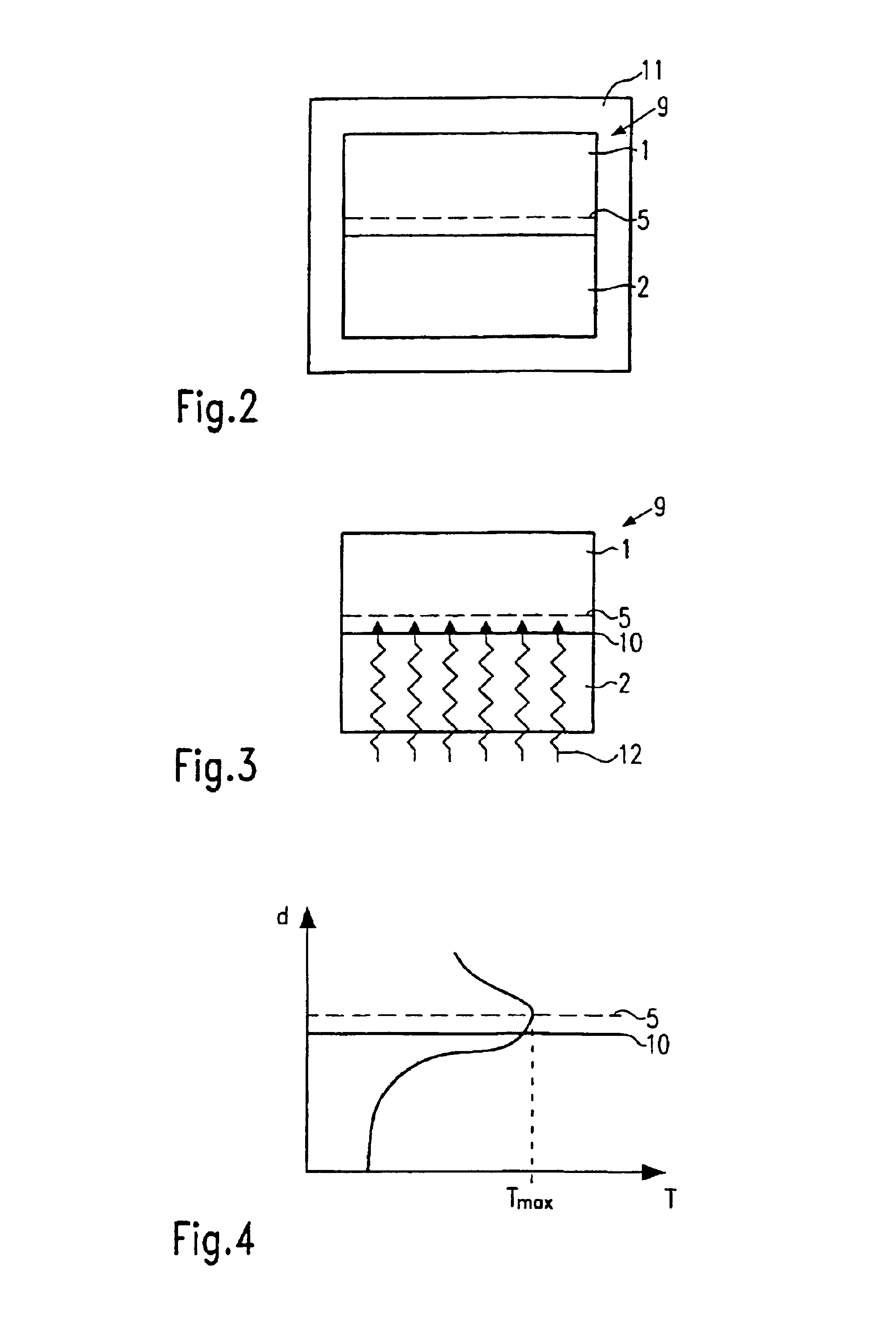
In accordance with one aspect of the invention, by annealing, the pre-determined detachment area of the heterogeneous material compound can be pre-fragilized thermally, yet not thermally detached at the detachment area. In this manner, a certain amount of thermal energy is already provided to this pre-determined detachment area as a result from annealing. Irradiation provides the additional amount of thermal energy needed to detach the heterogeneous material compound at the pre-determined and pre-fragilized detachment area in an easy but efficient way. It allows the localization of additional thermal energy at the pre-determined detachment area, whereby a risk of deformation due to annealing which could lead to damage or degradation of the heterogeneous material compound can be reduced. With irradiation it is possible to obtain detached parts of the heterogeneous material compound relatively quickly, with good quality and very low risk of an indefinite destruction or degradation of ...


PUM

PropertyMeasurementUnit
temperatureaaaaaaaaaa
wavelengthaaaaaaaaaa

Abstract

The present invention relates to a method of manufacturing a wafer in which a heterogeneous material compound is detached at a pre-determined detachment area of the compound, and the compound is subject to a thermal treatment. It is the object of the present invention to provide an easy and effective method of detachment a heterogeneous material compound with a reduced risk of an undefined breaking of the compound. The object is solved by a method wherein the thermal treatment includes annealing the compound, where the annealing is stopped before a detachment of the compound, and an irradiation of the compound with photons in order to obtain a detachment of the compound at the pre-determined detachment area.

Description

BACKGROUND1. Field of the InventionThe present invention relates to a method of manufacturing a wafer, in which a heterogeneous material compound is detached at a pre-determined detachment area of the compound, and the compound is subject to a thermal treatment.2. Background of the InventionHeterogeneous material compounds or heterostructures having a thin layer attached to a receiver substrate with a different thermal expansion coefficient have attained considerable industry attention in the fields of microelectronics, optoelectronics and micromechanics. Such structures can be fabricated using deposition processes based on electroplating, evaporation, spinning, etc. In other approaches, a bulk material is bonded to a receiver substrate and thereafter thinned down, either by a chemical mechanical polishing or by etching of the material. These methods mostly have a very low efficiency due to a lot of process steps and the resulting structures often cannot be produced with the require...

Claims


Application Information

Patent Timeline
Patent Type & Authority Patents(United States)
IPC IPC(8): H01L21/762H01L21/70H01L21/02H01L21/265H01L27/12
CPCH01L21/76254H01L21/185
Inventor MAURICE, THIBAUTCAYREFOURCQ, IANFOURNEL, FRANCK
Owner S O I TEC SILICON ON INSULATOR THECHNOLOGIES
Why Eureka
Try Eureka