Process for manufacturing a through insulated interconnection in a body of semiconductor material

a technology of semiconductor material and through insulation, which is applied in the direction of semiconductor devices, semiconductor/solid-state device details, electrical devices, etc., can solve the problems of limiting the applicability of this solution, inability to integrate active components, and inability to isolate through openings

Inactive Publication Date: 2005-01-04
STMICROELECTRONICS SRL +1
View PDF19 Cites 132 Cited by
  • Summary
  • Abstract
  • Description
  • Claims
  • Application Information

AI Technical Summary

Benefits of technology

An embodiment of the present invention provides a process that will enable a front-rear connection of a wafer of sem

Problems solved by technology

In the process described above, the biggest difficulties lie in insulating the through openings (deposition of oxides, nitrides or polymeric materials), in that they have a depth of several tens of microns and have substantially vertical walls.
In the above structure, the

Method used


Image

  • Process for manufacturing a through insulated interconnection in a body of semiconductor material
  • Process for manufacturing a through insulated interconnection in a body of semiconductor material
  • Process for manufacturing a through insulated interconnection in a body of semiconductor material

Examples


Embodiment Construction

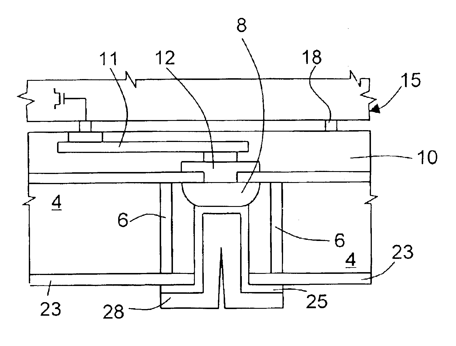
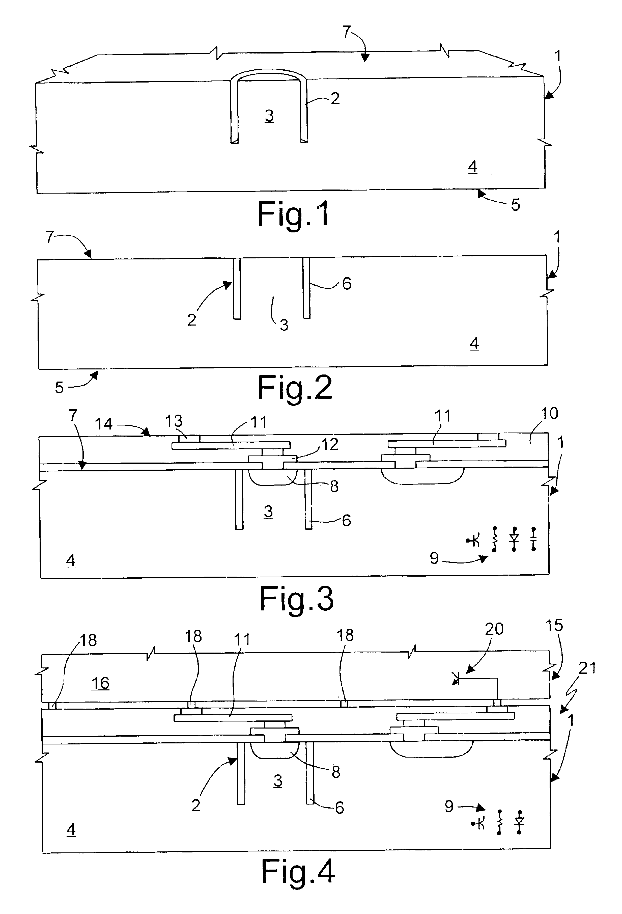
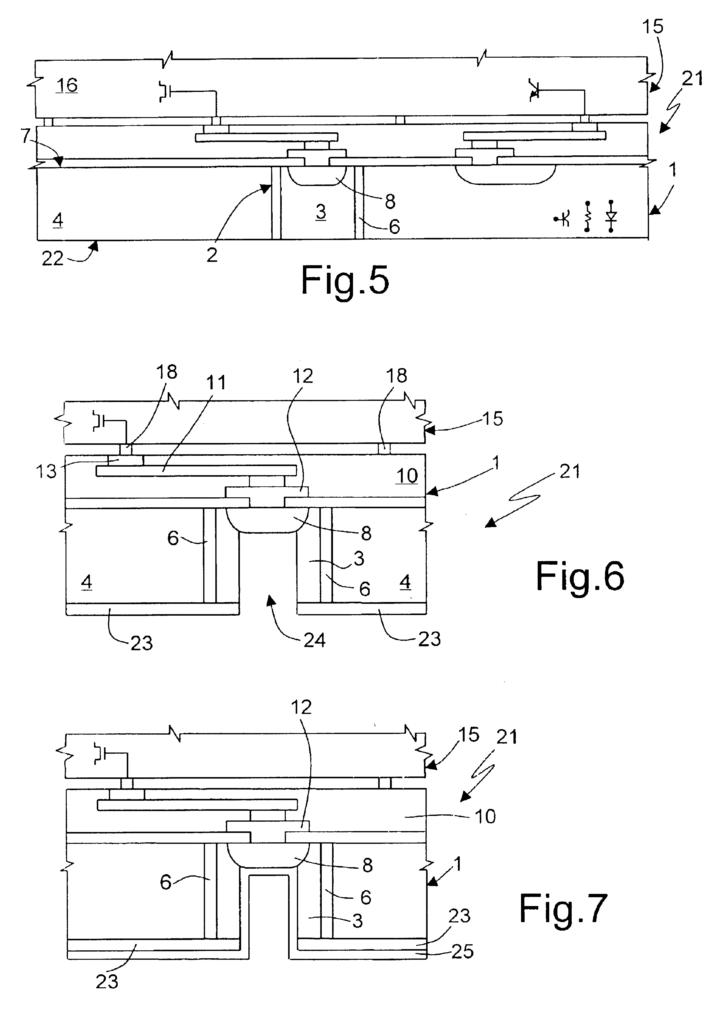
With reference to FIG. 1, a first wafer 1 comprising a substrate 4 of semiconductor material, typically monocrystalline silicon doped in a standard way, for example a P-type <100> substrate with a resistivity of 15 Ω / cm, having a first surface 7 and a second surface 5, has undergone steps for making trenches, according to what is described in the above-mentioned patent application EP-A-1 151 962 which is incorporated by reference. In particular, the first wafer 1 has been masked and etched to form deep trenches 2 having a closed shape and surrounding cylindrical regions 3 of monocrystalline silicon. The trenches 2 may have a depth of, for example, 50-100 μm.

Next (see FIG. 2), the trenches 2 are filled, either completely or partially, with insulating material 6, for example, silicon dioxide. For this purpose, a silicon dioxide layer is deposited or grown, and is then removed from the first surface 7 of the first wafer 1 to obtain the structure of FIG. 2.

In a known way (see FIG. ...


PUM


Abstract

The process for manufacturing a through insulated interconnection is performed by forming, in a body of semiconductor material, a trench extending from the front (of the body for a thickness portion thereof; filling the trench with dielectric material; thinning the body starting from the rear until the trench, so as to form an insulated region surrounded by dielectric material; and forming a conductive region extending inside said insulated region between the front and the rear of the body and having a higher conductivity than the first body. The conductive region includes a metal region extending in an opening formed inside the insulated region or of a heavily doped semiconductor region, made prior to filling of the trench.

Description

PRIORITYThis application claims priority from European patent application No. 02425207.4, filed Apr. 5, 2002, which is incorporated herein by reference.TECHNICAL FIELDThe present invention relates generally to a process for manufacturing a through insulated interconnection in a body of semiconductor material.BACKGROUND OF INVENTIONAs is known, for manufacturing microsystems comprising elements obtained using different technologies, such as microelectromechanical systems (MEMS) and integrated circuits, there exists the need to electrically connect two opposite faces (front and rear) of substrates integrating electronic components or, generally, carrying passive elements and / or protection structures and / or connection structures to other substrates.EP-A-0 926 723 describes a process for forming front-rear through contacts in micro-integrated electronic devices. According to this process, a metal contact region extends through a through opening in the chip. In detail, this process is ba...

Claims


Application Information

Patent Timeline
IPC IPC(8): H01L23/48H01L21/70H01L21/768
CPCH01L21/76898H01L23/481H01L2924/0002H01L2924/00014H01L2924/1461H01L2224/05572H01L2224/13025H01L2224/05009H01L2224/0401H01L2924/00012H01L2924/00H01L2224/05552
Inventor MASTROMATTEO, UBALDOFERRARI, PAOLO
Owner STMICROELECTRONICS SRL
Why Eureka
Try Eureka