Nonvolatile semiconductor memory device

a semiconductor memory and non-volatile technology, applied in static storage, digital storage, instruments, etc., can solve the problems of low threshold voltage of the core memory area, inability to properly execute read-out operations with fixed threshold voltage, and loss of charge in which the writing charge is not presen

Inactive Publication Date: 2005-01-04
INFINEON TECH LLC
View PDF3 Cites 38 Cited by
  • Summary
  • Abstract
  • Description
  • Claims
  • Application Information

AI Technical Summary

Benefits of technology

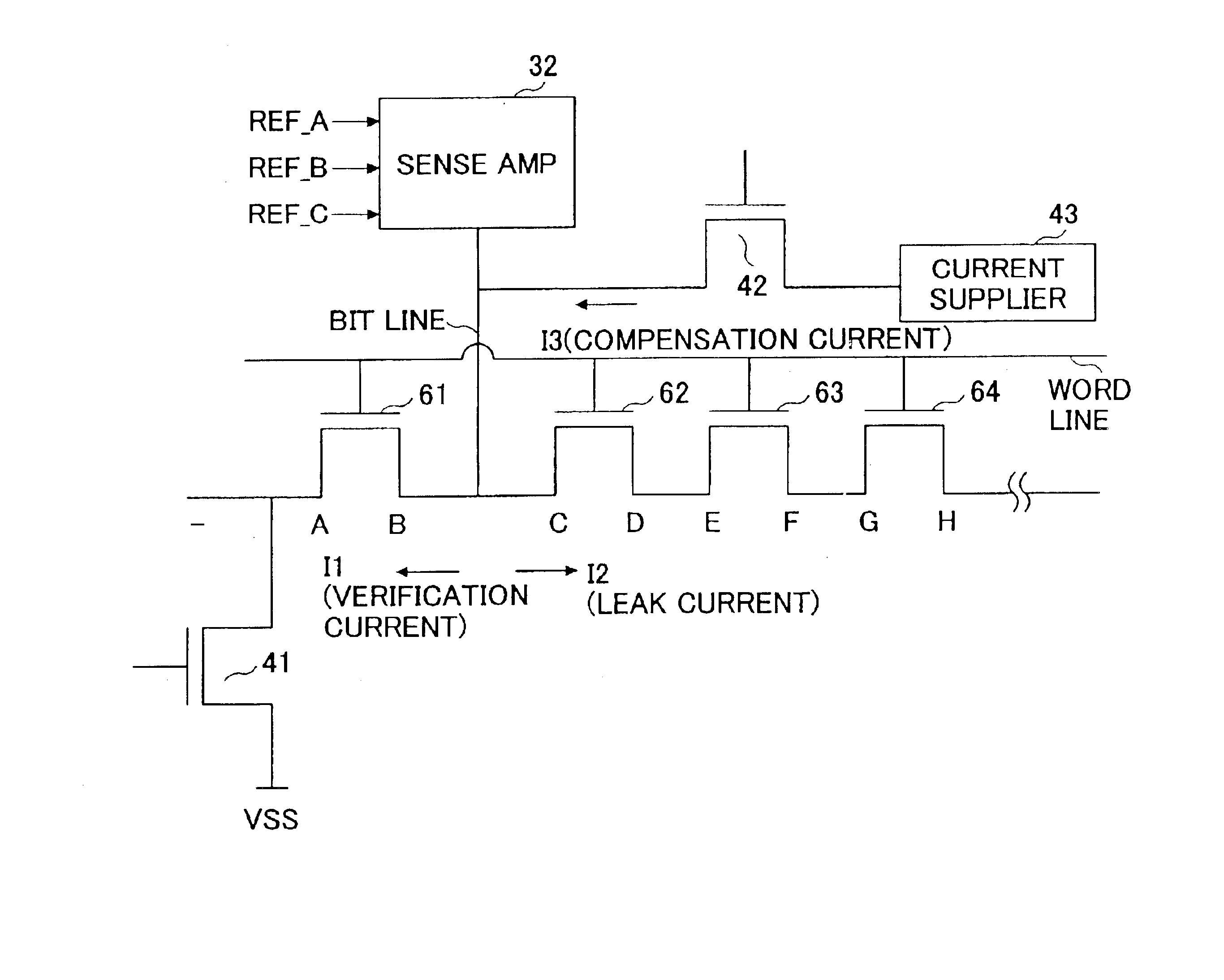
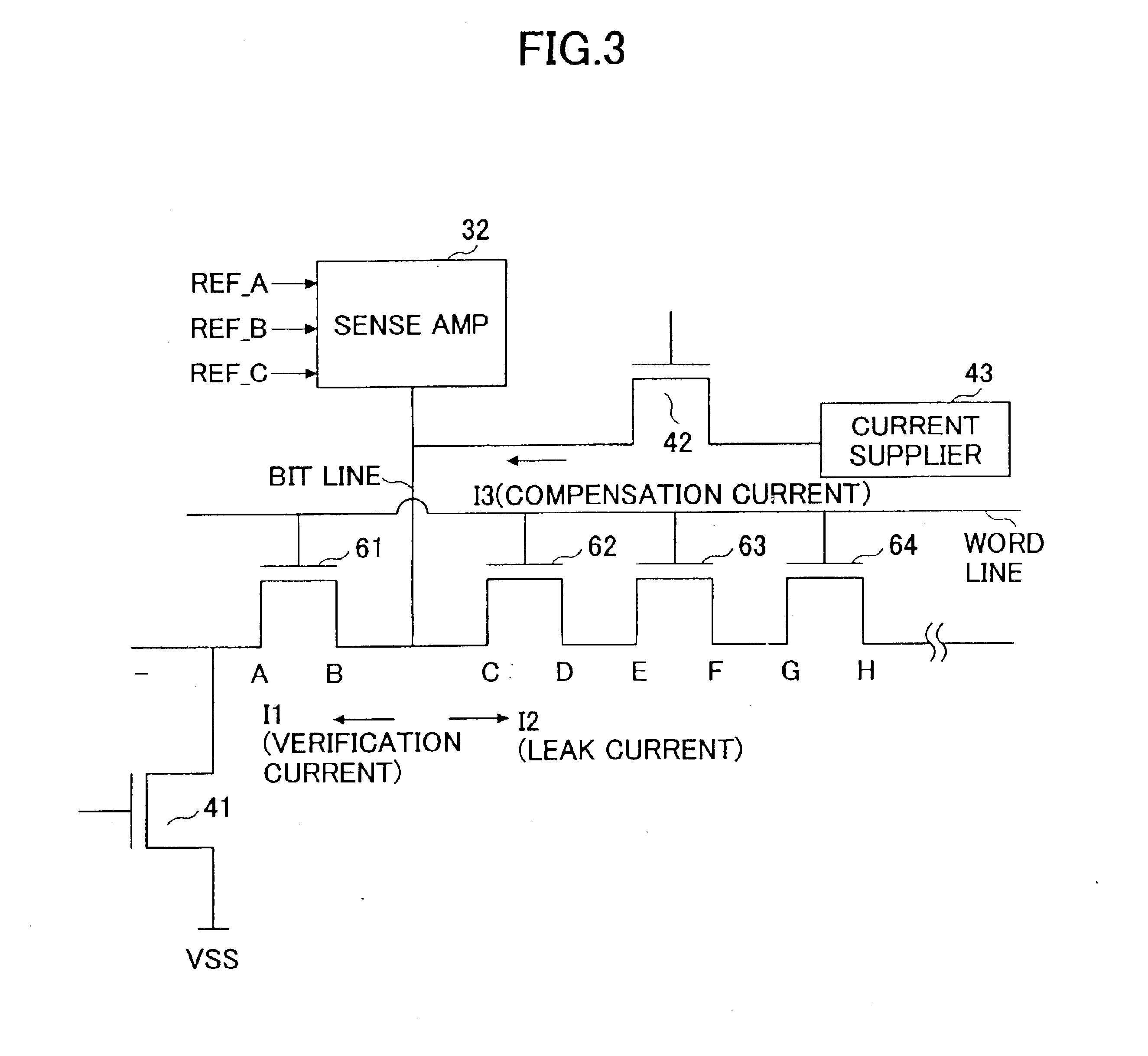
Therefore, according to the present invention, in the nonvolatile semiconductor memory device that is configured to use the average current of the two reference cells as the reference current, the influence by the leak current generated in the neighboring memory cell can be effectively reduced, and the detection of the exact program verification current of the target memory cell is possible.

Problems solved by technology

When the number of times of rewriting the memory cell in the nonvolatile semiconductor memory device increases, the charge loss in which the writing charge is lacked will occur, and it is in the tendency for the threshold level of the memory cell in the core memory area to become small.
For this reason, when the number of times of rewriting increases, the read-out operation is not properly executed with the fixed threshold voltage of the reference cell, and only an inadequate read-out margin is left for the read-out operation.
Therefore, only the lower limit is set up for the threshold level of the reference cell REF-0 programmed in the above manner, and it is uncertain whether the actually set threshold level is appropriate.
Similarly, only the upper limit is set up for the threshold level of the reference cell REF-1 programmed in the above manner, and it is uncertain whether the actually set threshold level is appropriate.
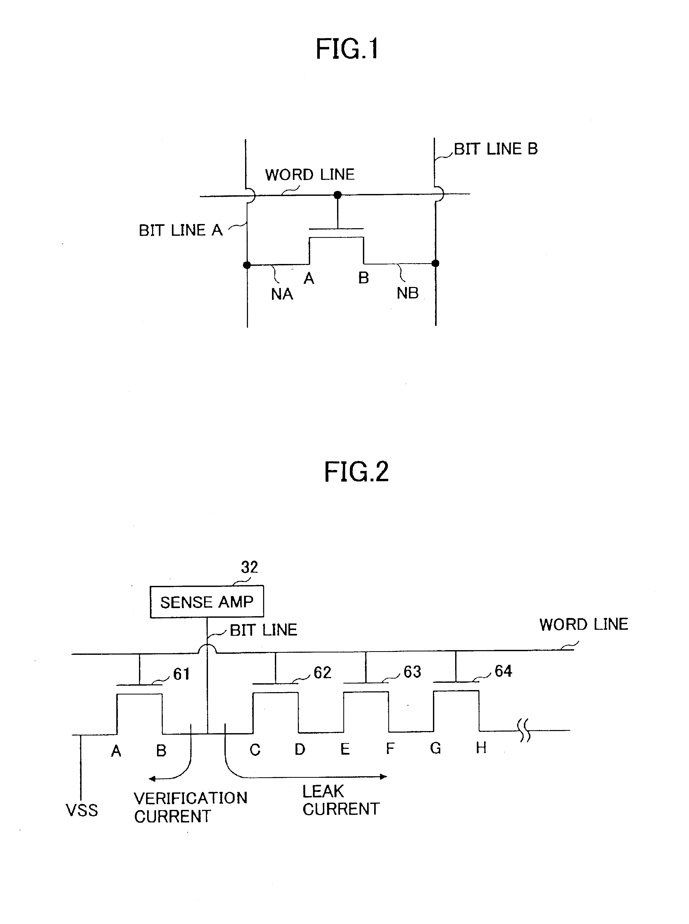
Hence, the leak current will occur in the neighboring memory cell due to the applied voltage.
If the leak current occurs, it is difficult to correctly detect the exact magnitude of the program verification current of the target memory cell.
The influence of the leak current of the neighboring memory cell 62 is given to the conventional nonvolatile semiconductor memory device without compensation, and the determination result of data is not reliable at the time of the comparison of the read-out current and the reference current.

Method used


Image

  • Nonvolatile semiconductor memory device
  • Nonvolatile semiconductor memory device
  • Nonvolatile semiconductor memory device

Examples


Embodiment Construction

A description will now be given of preferred embodiments of the present invention with reference to the accompanying drawings.

FIG. 4 shows the nonvolatile semiconductor memory device to which one preferred embodiment of the present invention is applied.

As shown in FIG. 4, the nonvolatile semiconductor memory device 10 of the present embodiment generally includes a control circuit 11, an I / O (input / output) buffer 12, an address latch 13, an X decoder (XDEC) 14, a Y decoder (YDEC) 15, a memory cell array 16, a data judging control circuit 17, a writing circuit 18, an erasing circuit 19, and a chip-enabling / output-enabling circuit 20.

The control circuit 11. receives the externally supplied control signals ( / WE, / CE), operates as a state machine based on the received control signals, and controls operation of each of the respective elements of the nonvolatile semiconductor memory device 10.

The input / output buffer 12 receives the externally supplied data, and supplies the received data t...


PUM


Abstract

A nonvolatile semiconductor memory device comprises a memory cell array which includes memory cells and reference cells, the reference cells including a first reference cell and a second reference cell. A data judging control unit generates an average reference current based on a first reference current from the first reference cell and a second reference current from the second reference cell, and determines data of each of the memory cells by comparison of a read-out current of each memory cell with the average reference current. A control unit performs a program verification operation to each memory cell. A compensation current supplying unit supplies a compensation current to a bit line of a target memory cell when a leak current of a neighboring memory cell adjacent to the target memory cell exceeds a predetermined reference value during the program verification operation.

Description

BACKGROUND OF THE INVENTION1. Field of the InventionThe present invention generally relates to a nonvolatile semiconductor memory device, and more particularly to a nonvolatile semiconductor memory device which uses a ferroelectric capacitor as a memory element at the time of read-out operation.2. Description of the Related ArtIn a nonvolatile semiconductor memory device, such as a flash memory, a reference current, read from a reference cell therein, is set to a predetermined threshold level (or a fixed reference level), and at the time of read-out operation, a drain current from a memory cell accessed therein is read out as the data, and the read-out current of the memory cell is compared with the reference current of the reference cell. The determination as to whether the data is “1” or “0” is performed depending on whether the read-out current is higher than the reference current or not.When the number of times of rewriting the memory cell in the nonvolatile semiconductor memory...

Claims


Application Information

Patent Timeline
Patent Type & Authority Patents(United States)
IPC IPC(8): G11C7/00G11C7/14G11C16/28G11C16/06G11C16/02
CPCG11C16/28G11C7/14
Inventor YAMADA, SHIGEKAZU
Owner INFINEON TECH LLC
Why Eureka
Try Eureka