Metal interconnection, semiconductor device, method for forming metal interconnection and method for fabricating semiconductor device

a metal interconnection and metal technology, applied in semiconductor devices, semiconductor/solid-state device details, electrical devices, etc., can solve the problems of reducing the reliability of the refractory metal film, the inability to use dry etching in patterning, and the limit to the improvement of the electro migration resistance near the interface, so as to improve the electro migration resistance and stress migration resistance, the effect of improving reliability

Inactive Publication Date: 2005-01-11
FUJITSU LTD
View PDF14 Cites 20 Cited by
  • Summary
  • Abstract
  • Description
  • Claims
  • Application Information

AI Technical Summary

Benefits of technology

An object of the present invention is to provide a metal interconnection, a semiconductor device, a method for forming a metal interconnection and a method for fabricating a semiconductor device which, when the

Problems solved by technology

In thus using Cu as an interconnection material, because Cu produces no halogenide of high vapor pressure, dry etching cannot be used in the patterning.
However, because of poor adhesion between the refractory metal film 103 and the Cu film 104, there is a limit to the imp

Method used


Image

  • Metal interconnection, semiconductor device, method for forming metal interconnection and method for fabricating semiconductor device
  • Metal interconnection, semiconductor device, method for forming metal interconnection and method for fabricating semiconductor device
  • Metal interconnection, semiconductor device, method for forming metal interconnection and method for fabricating semiconductor device

Examples


first embodiment

[A First Embodiment]

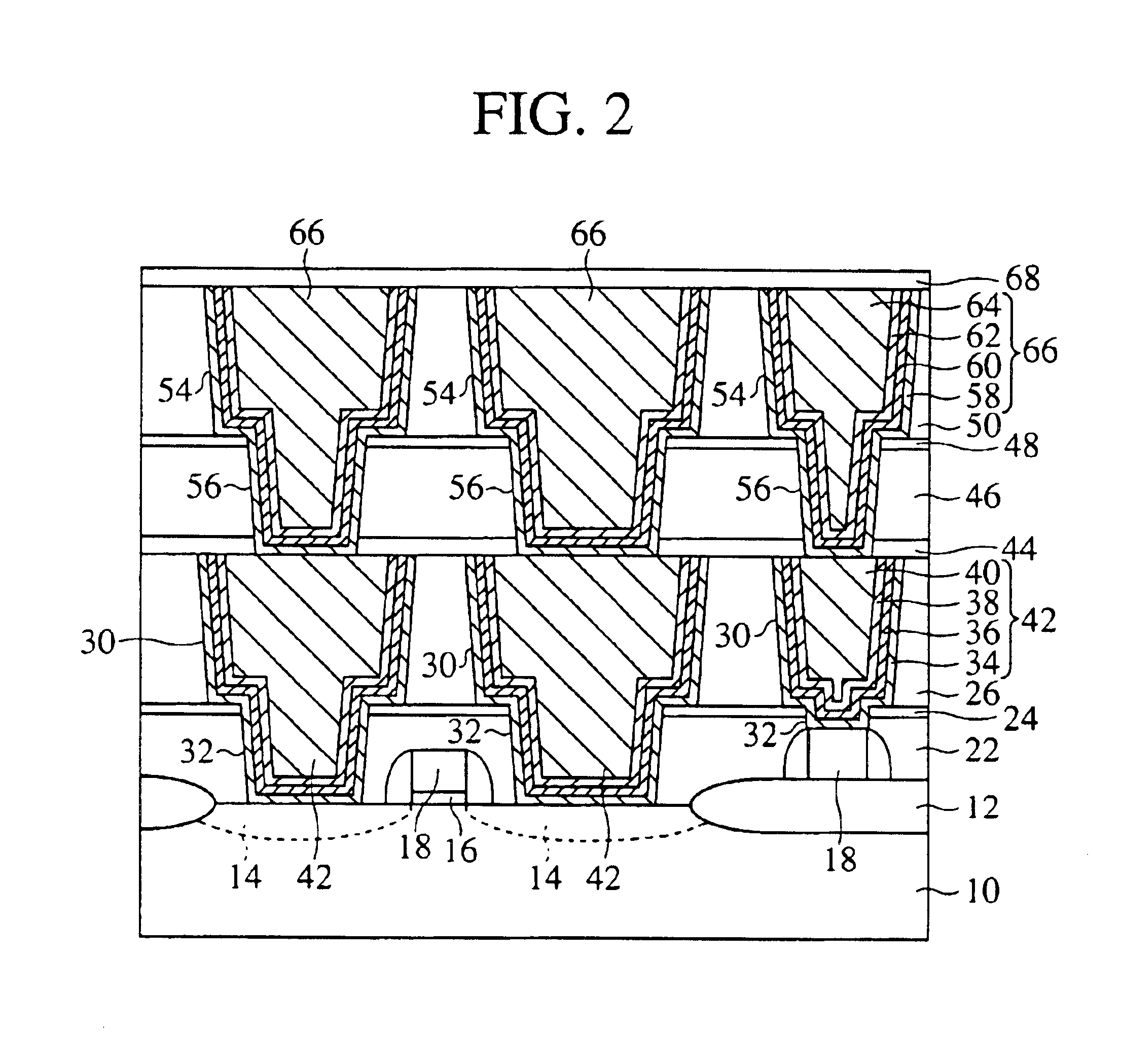
The semiconductor device and the method for fabricating the same according to a first embodiment of the present invention will be explained with reference to FIGS. 2, 3A-3D, 4A-4C, 5A-5C, 6A-6B, 7A-7B, 8A-8B and 9A-9B.

FIG. 2 is a diagrammatic sectional view of the semiconductor device according to the present embodiment, which shows a structure thereof. FIGS. 3A-3D, 4A-4C, 5A-5C, 6A-6B, 7A-7B, 8A-8B and 9A-9B are sectional views of the semiconductor device according to the present embodiment in the steps of the method for fabricating the same, which explain the method.

First, the structure of the semiconductor device according to the present embodiment will be explained with reference to FIG. 2.

A MOS transistor including a source / drain diffused layer 14 and a gate electrode 18 is formed in a device region of a silicon substrate 10 defined by a device isolation film 12.

On the silicon substrate 10 with the MOS transistor formed on, there are formed an inter-layer in...

second embodiment

[A Second Embodiment]

The method for fabricating the semiconductor device according to a second embodiment of the present invention will be explained with reference to FIGS. 2, 3A-3D, 4A-4C, 5A-5C, 6A-6B, 7A-7B, 8A-8B and 9A-9B. The same members of the present embodiment as those of the first embodiment are represented by the same reference numbers not to repeat or to simplify their explanation.

FIG. 2 is a diagrammatic sectional view of the semiconductor device according to the present embodiment, which show a structure thereof. FIGS. 3A-3D, 4A-4C, 5A-5C, 6A-6B, 7A-7B, 8A-8B and 9A-9B are sectional view of the semiconductor device according to the present embodiment in the steps of the method for fabricating the same, which explain the method.

The semiconductor device according to the present embodiment and the method for fabricating the semiconductor device are the same as those according to the first embodiment except the method for forming the barrier layer, the adhesion layer and ...

third embodiment

[A Third Embodiment]

The semiconductor device and the method for fabricating the same according to a third embodiment of the present invention will be explained with reference to FIGS. 10, 11A-11C, 12A-12C, 13A-13B and 14A-14B. The same member of the present embodiment as those of the semiconductor device according to the first and the second embodiments and the method for fabricating the same are represented by the same reference numbers not to repeat or to simplify their explanation.

FIG. 10 is a diagrammatic sectional view of the semiconductor device according to the present embodiment, which shows a structure thereof. FIGS. 11A-11C, 12A-12C, 13A-13B and 14A-14B are sectional views of the semiconductor device in the steps of the method for fabricating the semiconductor device, which show the method.

The semiconductor device according to the present embodiment has the adhesion between the inter-layer insulation film and the barrier layer improved. The semiconductor device and the met...


PUM


Abstract

A semiconductor device comprising: a base substrate including a semiconductor substrate 10 and a semiconductor element formed on the semiconductor substrate 10; an insulation film 22, 24, 26 formed on the base substrate having an opening 30, 32; and a metal interconnection 42 formed buried in the opening 30, 32 including: a barrier layer 34 formed on an inside wall and a bottom of the opening 30, 32; an adhesion layer 36 containing zirconium formed on the barrier layer 34; and a metal interconnection material 38, 40 containing copper as a main component formed on the barrier layer 36. Whereby the peeling of the copper interconnection in the fabrication process can be prevented. The electro migration resistance and stress migration resistance of the copper interconnection can be further improved.

Description

CROSS-REFERENCE TO RELATED APPLICATIONSThis application is based upon and claims priority of Japanese Patent Applications Nos. Hei 11-240866, 2000-169361, and 2000-236744, all filed, the contents being incorporated herein by reference.BACKGROUND OF THE INVENTIONThe present invention relates to an interconnection used in semiconductor devices, etc., more specifically to an interconnection which is suitably applicable to metal interconnections, semiconductor devices, methods for forming the metal interconnection and methods for fabricating the semiconductor devices which use Cu (copper) for lower resistivity.As semiconductor integrated circuits have been recently higher integrated, elements formed on the semiconductor substrates and interconnections connecting the elements have been increasingly micronized. Accordingly, characteristics and reliability required of the interconnections have become stricter. More reliable interconnection materials having lower resistivity, electro migrat...

Claims


Application Information

Patent Timeline
IPC IPC(8): H01L21/70H01L23/532H01L21/768H01L23/52H01L21/304H01L21/306H01L21/3205
CPCH01L21/7681H01L21/76846H01L21/76858H01L23/53238H01L21/76873H01L21/76874H01L23/53233H01L21/76868H01L2924/0002H01L2924/00H01L21/768
Inventor UCHIBORI, CHIHIRO
Owner FUJITSU LTD
Why Eureka
Try Eureka