

Three-dimensional device
a three-dimensional device and device technology, applied in the direction of superconductor details, instruments, transistors, etc., can solve the problems of specific substrates and difficult to form individual layers with suitable device parameters, and achieve the effect of flexible formation and easy formation
- Summary
- Abstract
- Description
- Claims
- Application Information
AI Technical Summary
Benefits of technology
Problems solved by technology
Method used
Image

Examples
Embodiment Construction
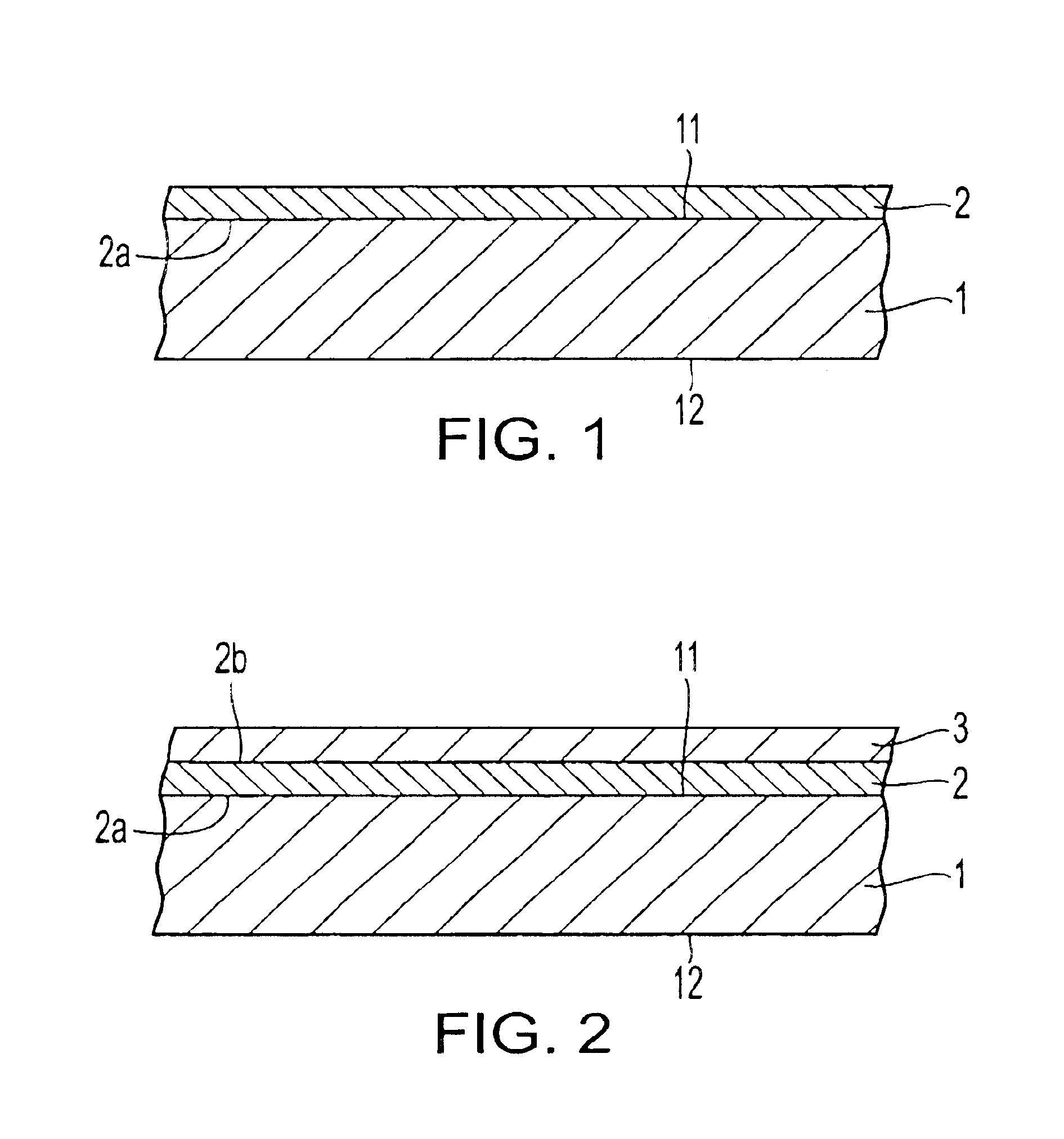
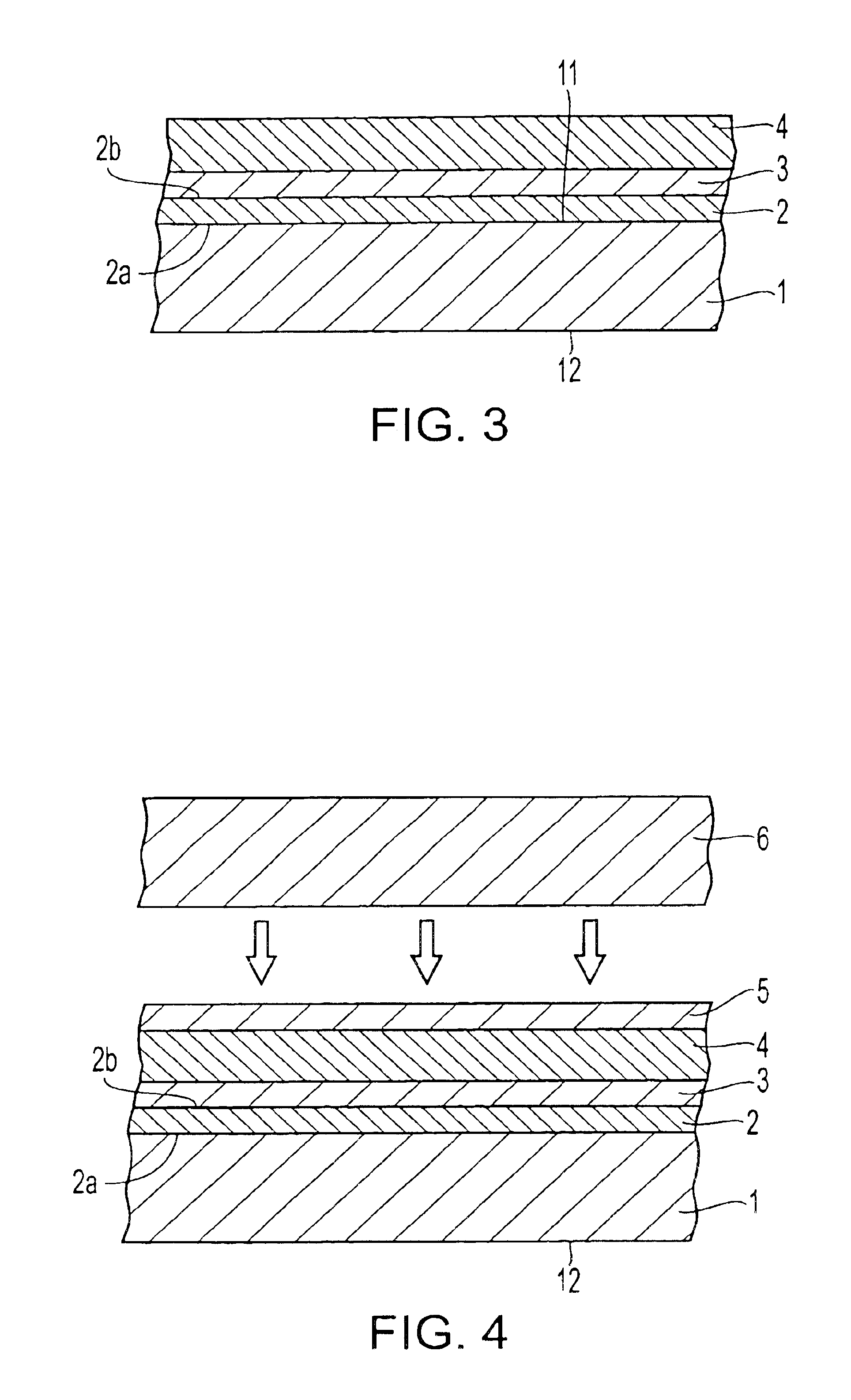
e-dimensional device in the present invention.
[0050]FIG. 19 is a sectional view which shows an example of a configuration of an organic EL device in the present invention.
[0051]FIG. 20 is a sectional view which shows an example of a configuration of a PIN photodiode in the present invention.
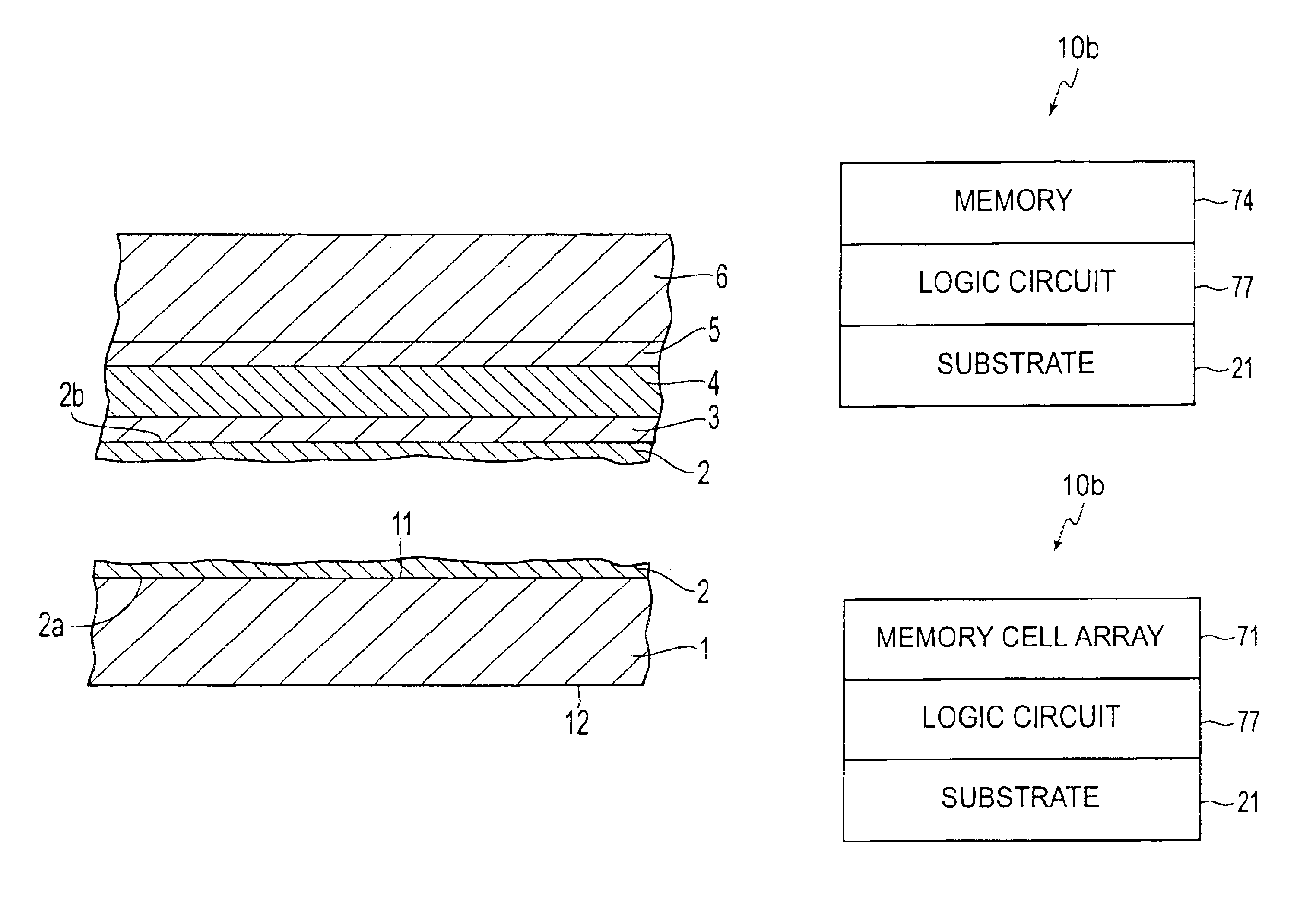
[0052]FIG. 21 is a sectional view which schematically shows a fourth example of a three-dimensional device in the present invention.
[0053]FIG. 22 is a circuit diagram which shows an example of a configuration of a memory cell (one cell) of an SRAM in the present invention.
[0054]FIG. 23 is a perspective view which schematically shows a fifth example of a three-dimensional device in the present invention.
[0055]FIG. 24 is a perspective view which schematically shows a sixth example of a three-dimensional device in the present invention.
[0056]FIG. 25 is a schematic diagram which shows a seventh example of a three-dimensional device in the present invention.
[0057]FIG. 26 is a schematic diagram which s...
PUM
| Property | Measurement | Unit |
|---|---|---|
| temperature | aaaaa | aaaaa |
| thickness | aaaaa | aaaaa |
| thickness | aaaaa | aaaaa |
Abstract
Description
Claims
Application Information