Micro-scale interconnect device with internal heat spreader and method for fabricating same

Inactive Publication Date: 2005-01-25
AAC TECH PTE LTD
View PDF2 Cites 68 Cited by
  • Summary
  • Abstract
  • Description
  • Claims
  • Application Information

AI Technical Summary

Benefits of technology

It is therefore an object of the invention to provide a micro-scale interconnect device with an internal heat spreader and related methods of fabrication and use.

Problems solved by technology

However, the electrical current carried through a high-density interconnect arrangement of communication lines can give rise to self-heating.
The heat energy dissipated through a micro-scale structure, particularly a MEMS device built over an interconnect scheme, can damage the components of the structure or impair the performance of those components.
Depending on the current load, the elevated temperatures attained can result in thermally induced stress-related issues such as warping.
A thermally-induced curvature in the substrate of this MEMS device could result in the shorting of the DC switch.
As another example, in the case of very high current loads that are likely to occur during a power surge, the temperatures attained could be high enough to heat certain materials of a micro-scale device up to their melting point or transition temperature, and thus cause destruction of the entire device.
Thus, while it is desirable to integrate a high-density interconnect scheme with a micro-scale device, the inclusion of the interconnect scheme would restrict the operating range of the device and raise concerns about the reliability of the device.

Method used


Image

  • Micro-scale interconnect device with internal heat spreader and method for fabricating same
  • Micro-scale interconnect device with internal heat spreader and method for fabricating same
  • Micro-scale interconnect device with internal heat spreader and method for fabricating same

Examples


Embodiment Construction

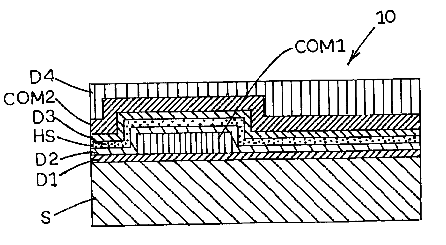
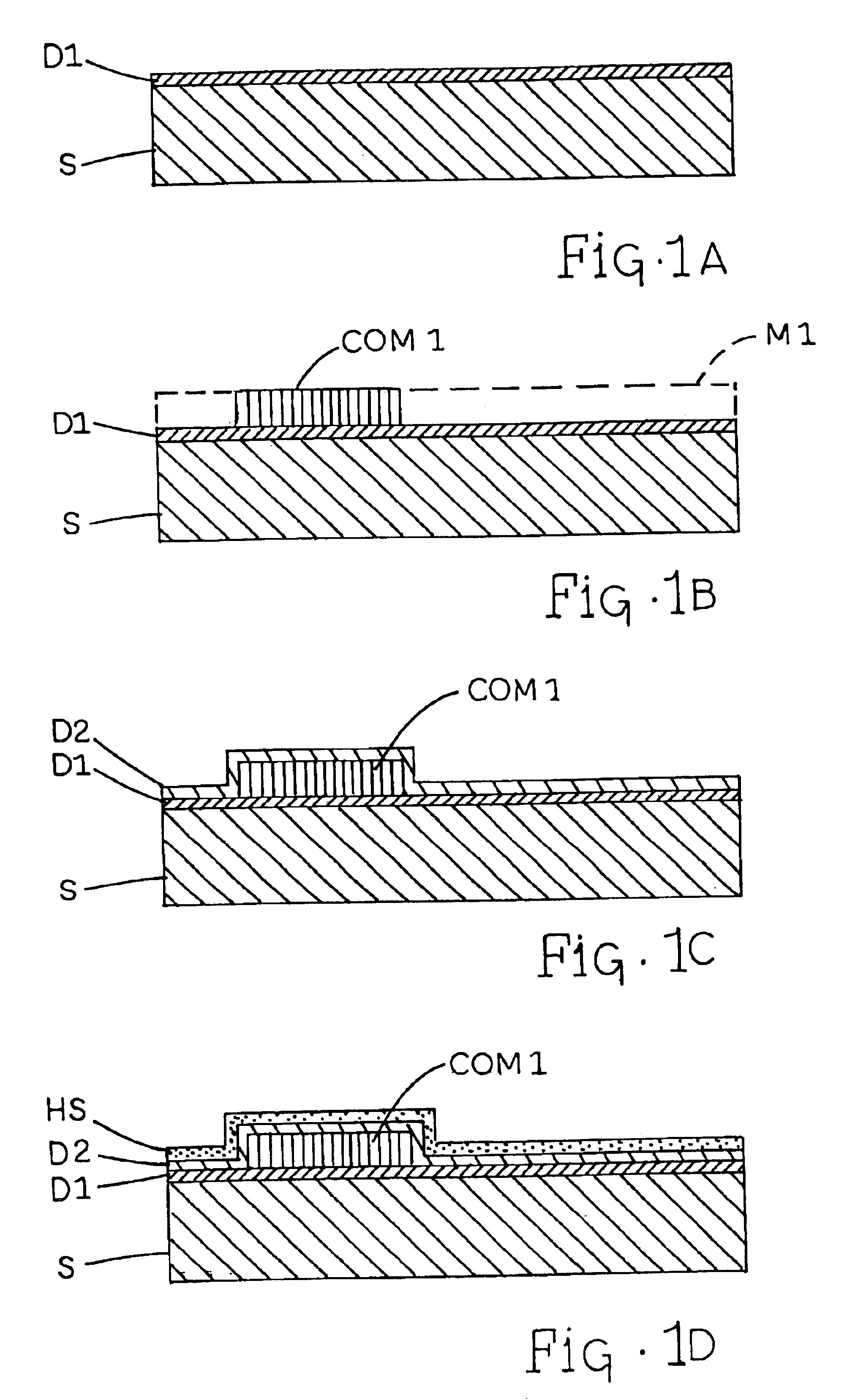
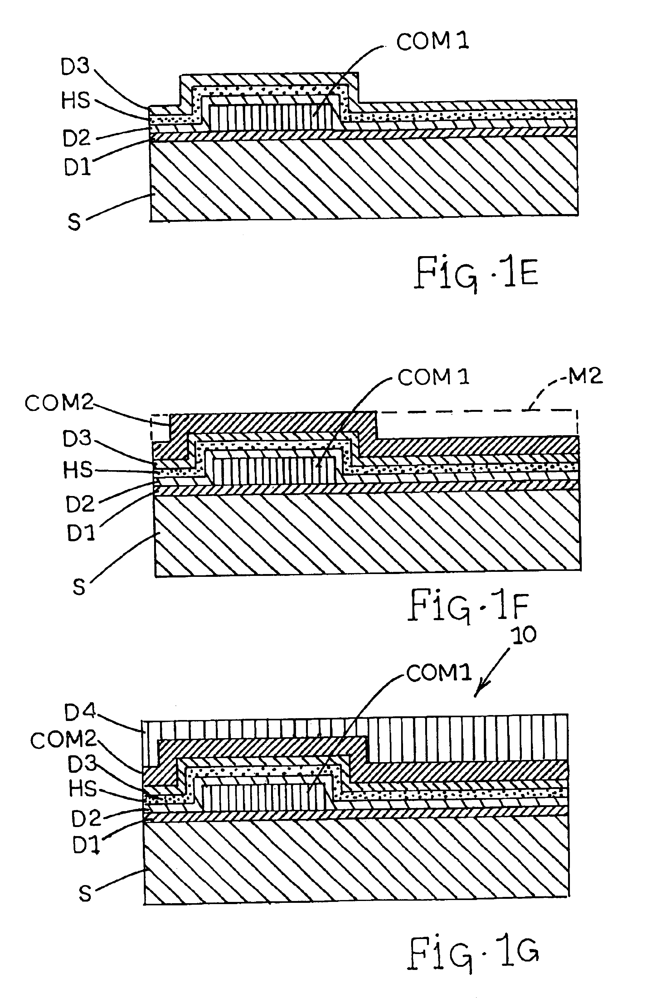
For purposes of the present disclosure, it will be understood that when a given component such as a layer, film, region or substrate is referred to herein as being disposed or formed “on” another component, that given component can be directly formed on the other component or, alternatively, intervening components (for example, one or more buffer, transition or lattice-matching layers, interlayers, adhesion or bonding layers, electrodes or contacts) can also be present. It will be further understood that the terms “disposed on” and “formed on” are used interchangeably to describe how a given component is positioned or situated in relation to another component. Moreover, terms such as “disposed on” and “formed on” are not intended to introduce any limitations relating to particular methods of material deposition, film growth, or other fabrication techniques.

For the purpose of the present disclosure, the term “layer” denotes a generally thin, two-dimensional structure having an out-of...


PUM

PropertyMeasurementUnit
Thicknessaaaaaaaaaa
Thicknessaaaaaaaaaa
Widthaaaaaaaaaa

Abstract

A micro-scale interconnect device with internal heat spreader and method for fabricating same. The device includes first and second arrays of generally coplanar electrical communication lines. The first array is disposed generally along a first plane, and the second array is disposed generally along a second plane spaced from the first plane. The arrays are electrically isolated from each other. Embedded within the interconnect device is a heat spreader element. The heat spreader element comprises a dielectric material disposed in thermal contact with at least one of the arrays, and a layer of thermally conductive material embedded in the dielectric material. The device is fabricated by forming layers of electrically conductive, dielectric, and thermally conductive materials on a substrate. The layers are arranged to enable heat energy given off by current-carrying communication lines to be transferred away from the communication lines.

Description

TECHNICAL FIELDThe present invention generally relates to micro-scale electrical interconnect devices and the fabrication thereof. More particularly, the present invention relates to the integration of heat spreading elements with such interconnect devices.BACKGROUND ARTMicro-scale devices or systems such as integrated circuits (ICs), opto-electronic and photonic devices, micromechanical devices, micro-electro-mechanical systems (MEMS), micro-opto-electro-mechanical systems (MOEMS or optical MEMS), chip-based biosensors and chemosensors, microfluidic devices (e.g., labs-on-a-chip), and other articles characterized by micron- and sub-micron-sized features often require the use of high-density electrical interconnect schemes for transmitting signals. The interconnect scheme can consist of a cross-bar array of communication lines located at different levels or planes of a micro-scale structure. For example, one level can contain an arrangement of parallel input lines, while another lev...

Claims


Application Information

Patent Timeline
IPC IPC(8): B81B3/00H01H61/00H01L23/373H01L23/522H01H61/04H01L23/52H01L23/34H02N10/00H01H1/50H01H1/02H01H1/00H01H1/04H01L27/12B81B7/00H01H59/00H01L21/302H01L29/86H02N1/00
CPCB81B3/0024B81C1/0015H01H59/0009H01H61/04H01L23/3735H01L23/522H02N1/006H02N10/00B81B3/0051Y10T29/49222B81B2201/014B81B2201/018B81B2203/0118B81B2203/04B81B2207/07B81C2201/0107B81C2201/0108B81C2201/0109H01H1/04H01H1/504H01H2001/0042H01H2001/0063H01H2001/0089H01H2059/0072H01H2061/006H01L27/1203H01L2924/09701H01L2924/0002H01L2924/00
Inventor SETT, SUBHAMCUNNINGHAM, SHAWN JAY
Owner AAC TECH PTE LTD
Why Eureka
Try Eureka