Non-volatile semiconductor memory device reading and writing multi-value data from and into pair-cells

a non-volatile, memory device technology, applied in the direction of color television, instruments, television systems, etc., can solve the problems of large power consumption, small power consumption of conventional nand-type flash memory,

Inactive Publication Date: 2005-01-25
KK TOSHIBA
View PDF4 Cites 92 Cited by
  • Summary
  • Abstract
  • Description
  • Claims
  • Application Information

AI Technical Summary

Problems solved by technology

In addition, since NAND-type flash memory is possible to be written into plural cells at a time by FN tunneling, power consumption thereof is small.
On the other hand, NOR-type flash memory is characterized in that it is high-speed accessible, while the power consumption is large because hot electron injection is used for data writing.
However, recent mobile devices are going to treat image data and the like with large data quantities.
As described above, a conventional NAND-type flash memory, cell current of which is small due to its NAND string structure, is not suitable for high-speed random accessing.
Even if the above-described method is used, the performance improvement of the conventional NAND flash memory is limited.
However, this approach will dilute a property of the NAND-type flash memory as the unit cell area is small.
It is not practical to statically make a reference current with about a half of the on-cell current for each bit line pair.

Method used


Image

  • Non-volatile semiconductor memory device reading and writing multi-value data from and into pair-cells
  • Non-volatile semiconductor memory device reading and writing multi-value data from and into pair-cells
  • Non-volatile semiconductor memory device reading and writing multi-value data from and into pair-cells

Examples


Embodiment Construction

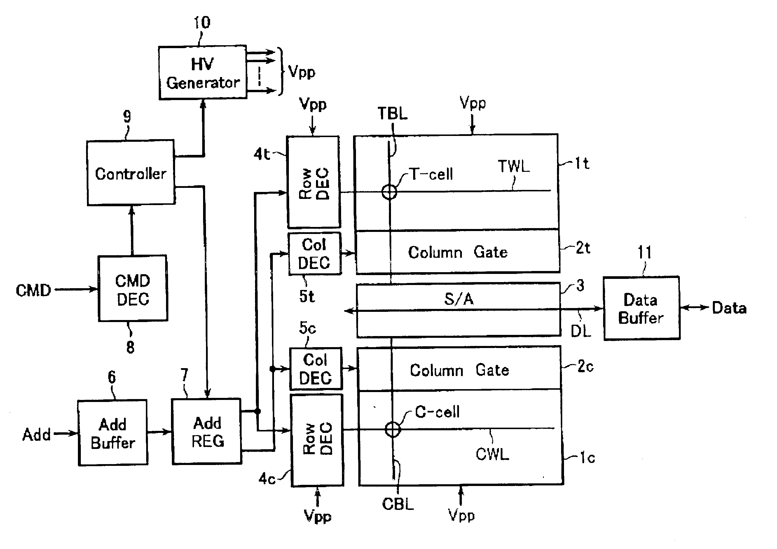
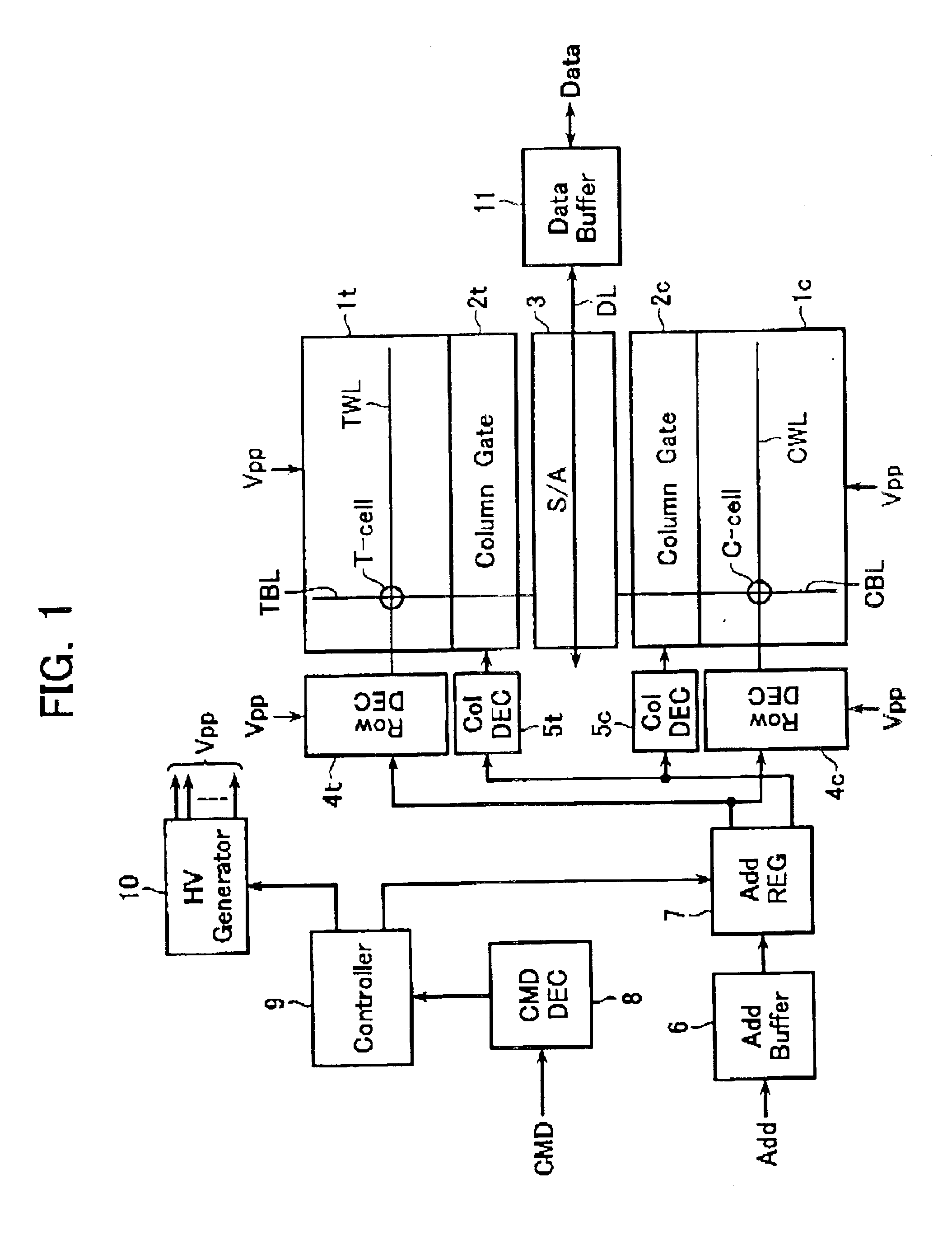
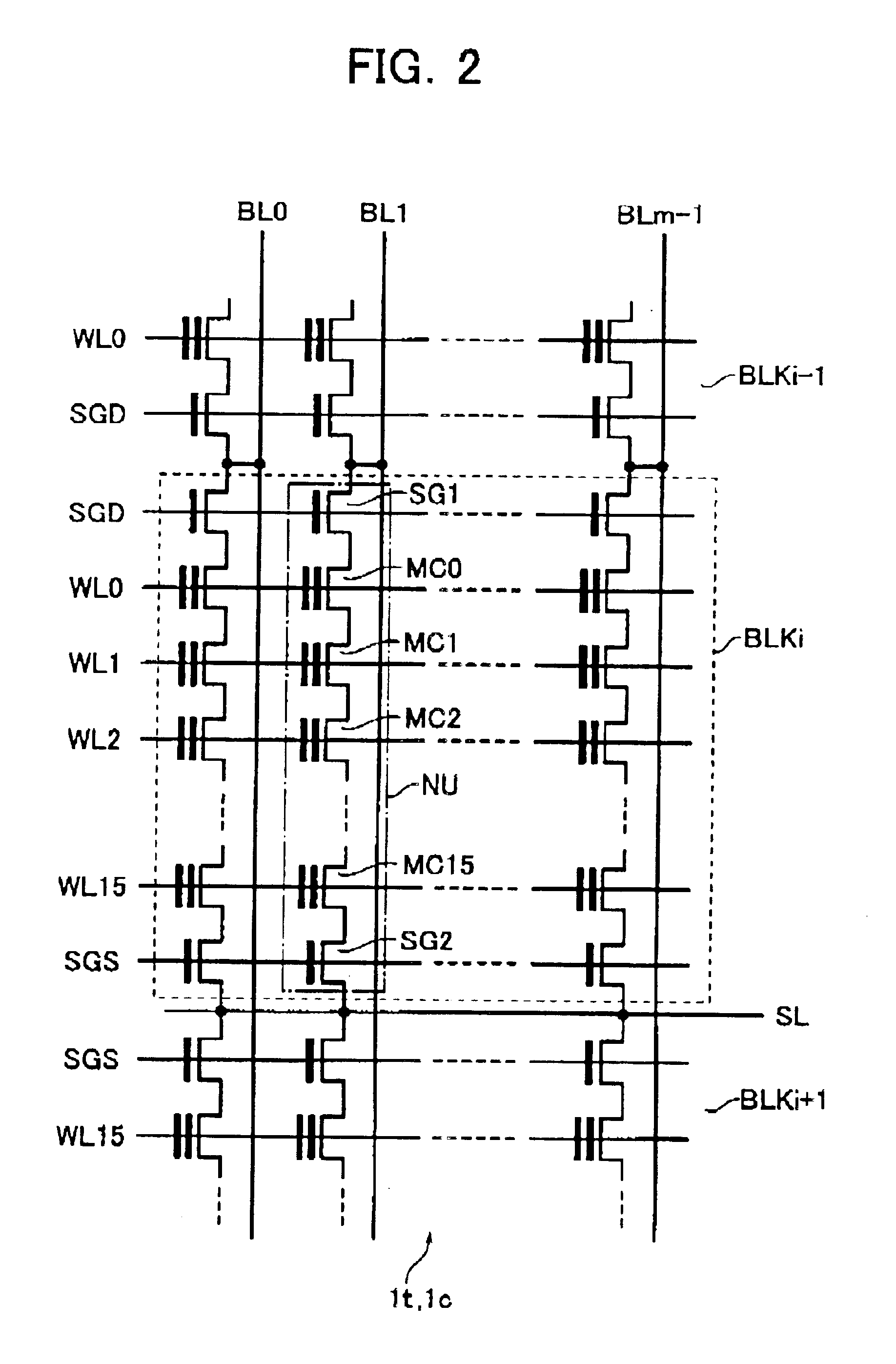
[0037]Referring to the drawings, a NAND-type flash memory according to an embodiment will be described bellow. In the flash memory of this embodiment, a combination of a multi-value data storage scheme and a pair-cell scheme, in which two cells constitute a pair-cell for storing complementary data therein, is used. By use of the above-described combination of two schemes, it is able to achieve a NAND memory system with a high-speed performance while bit density thereof is maintained at a high level. That is, in the pair-cell scheme, data storage is performed by one-bit / two-cell. In this case, however, perform for example 4-value data storage for a pair-cell, and it results in a storage manner of one-bit / one-cell. Further, perform data determination by comparing two cell currents for each pair-cell, it becomes to be able to precisely read out data with a high-speed performance even if the cell current is small.

[0038]It should be appreciated that this invention may be generally applie...


PUM


Abstract

A non-volatile semiconductor memory device includes: a memory cell array in which a plurality of electrically rewritable and non-volatile memory cells are arranged; a sense amplifier circuit configured to write M-value data (where, M is an integer equal to 4 or more) to pair-cells each constituted by simultaneously selected first and second memory cells connected to a pair of bit lines in the memory cell array, the M-value data being defined as a combination of different threshold levels of the first and second memory cells in M threshold levels to be set at each memory cell, and read M-value data stored in each pair-cell by sensing a difference between cell currents of the first and second memory cells; and a controller configured to control data write and read operations for the memory cell array.

Description

CROSS-REFERENCE TO RELATED APPLICATION[0002]This application is based on and claims the benefit of priority from the prior Japanese Patent Application No. 2003-111960, filed on Apr. 16, 2003, the entire contents of which are incorporated herein by reference.BACKGROUND OF THE INVENTION[0003]1. Field of the Invention[0004]This invention relates to an electrically rewritable and non-volatile semiconductor memory device (EEPROM) and an electric device using the same.[0005]2. Description of Related Art[0006]EEPROM flash memories are roughly classified into two types, i.e., NAND-type and NOR-type. A NAND-type flash memory uses a NAND string (i.e., NAND cell unit) with plural cells serially connected as sharing sources and drains with the neighboring cells. Due to this fact, the NAND-type flash memory has a higher cell density than a NOR-type flash memory. In addition, since NAND-type flash memory is possible to be written into plural cells at a time by FN tunneling, power consumption ther...

Claims


Application Information

Patent Timeline
Patent Type & Authority Patents(United States)
IPC IPC(8): G11C16/02G06K19/07G11C16/04G11C16/28G11C16/06H04N5/907G11C7/06G11C11/34G11C11/56
CPCG11C7/065G11C11/5628G11C11/5642G11C16/26G11C16/28G11C16/3459G11C16/0483G11C2211/5621
Inventor TODA, HARUKI
Owner KK TOSHIBA
Why Eureka
Try Eureka