Check patentability & draft patents in minutes with Patsnap Eureka AI!

Synchronous SRAM-compatible memory device including DRAM array with internal refresh

a memory device and synchronous technology, applied in static storage, information storage, digital storage, etc., can solve the problems of increasing the unit cost of an sram, deteriorating the entire performance of a system, and disadvantageous requirements of sram, so as to achieve effective input in synchronization

Inactive Publication Date: 2005-01-25
MOSAID TECH
View PDF5 Cites 13 Cited by
  • Summary
  • Abstract
  • Description
  • Claims
  • Application Information

AI Technical Summary

Benefits of technology

In an embodiment of the present invention, the synchronous SRAM-compatible memory including a DRAM array composed of a plurality of DRAM cells arranged in a matrix form defined by rows and columns. The DRAM cells require a refresh operation at regular intervals to maintain data stored in the synchronous SRAM-compatible memory. The synchronous SRAM-compatible memory interfaces with an external system for simultaneously providing a row address and a column address. The synchronous SRAM-compatible memory includes the DRAM array; a data input / output unit for controlling input and output of data to / from the DRAM array; an address input unit for inputting a row address and a column address of a current frame in a range where a certain effective address signal is activated, the addresses being effectively input in synchronization with a certain external clock signal; a burst address generating unit for generating a burst address sequentially varying with respect to the column address in synchronization with the external clock signal; a state control unit for generating a burst enable signal that enables the burst address generating unit, controlling the data input / output unit, and generating a wait indication signal of a first logic state while an access operation of a previous frame is performed with respect to the DRAM array, the access operation of the previous frame including a write access operation and a refresh operation before the effective address signal of the current frame is activated; a refresh timer for generating a refresh request signal activated at regular intervals; and a refresh control unit for controlling the refresh operation with respect to the DRAM array in response to the refresh request signal, the refresh operation being performed after completion a the burst access operation ongoing with respect to the DRAM array.
In accordance with the present invention, a method of driving a synchronous SRAM-compatible memory is provided. The method of the synchronous SRAM-compatible memory includes the steps of (A) inputting an effective address signal, in which the row and column addresses of the current frame are effectively input while the effective address signal is activated, and the row and column addresses of the current frame are not effectively input while the effective address signal is inactivated; (B) determining whether an access operation of a previous frame is performed when activation of the effective address signal is detected; (C) waiting for completion of the access operation of the previous frame and generating a wait indication signal of a first logic state to provide the wait indication signal to an outside when it is determined that the access operation of the previous frame is performed in the step (B); and (D) performing a burst access operation in which a burst address for selecting a column of the DRAM memory array is varied in synchronization with an external clock signal when it is determined that the access operation of the previous frame is completed in the step (B). The access operation of the previous frame includes a write access operation and a refresh operation generated before the effective address signal of the current frame is activated.

Problems solved by technology

However, since each unit memory cell of the SRAM is composed of six transistors, the SRAM disadvantageously requires a large wafer area compared to a DRAM in which each unit memory cell is implemented using a transistor and a capacitor.
Such a large wafer area increases the unit cost of an SRAM.
Further, the entire performance of a system is deteriorated due to the time required to perform the refresh operation and a slow operation speed.
However, in the conventional technology, since a column address is continuously changed even though a column address is not received from the outside in the state where a word line for selecting a row of a memory array is kept activated, the burst access operation of inputting / outputting data to / from a specified memory cell cannot be implemented.

Method used


Image

  • Synchronous SRAM-compatible memory device including DRAM array with internal refresh
  • Synchronous SRAM-compatible memory device including DRAM array with internal refresh
  • Synchronous SRAM-compatible memory device including DRAM array with internal refresh

Examples


Embodiment Construction

Reference now should be made to the drawings, in which the same reference numerals are used throughout the different drawings to designate the same or equivalent components.

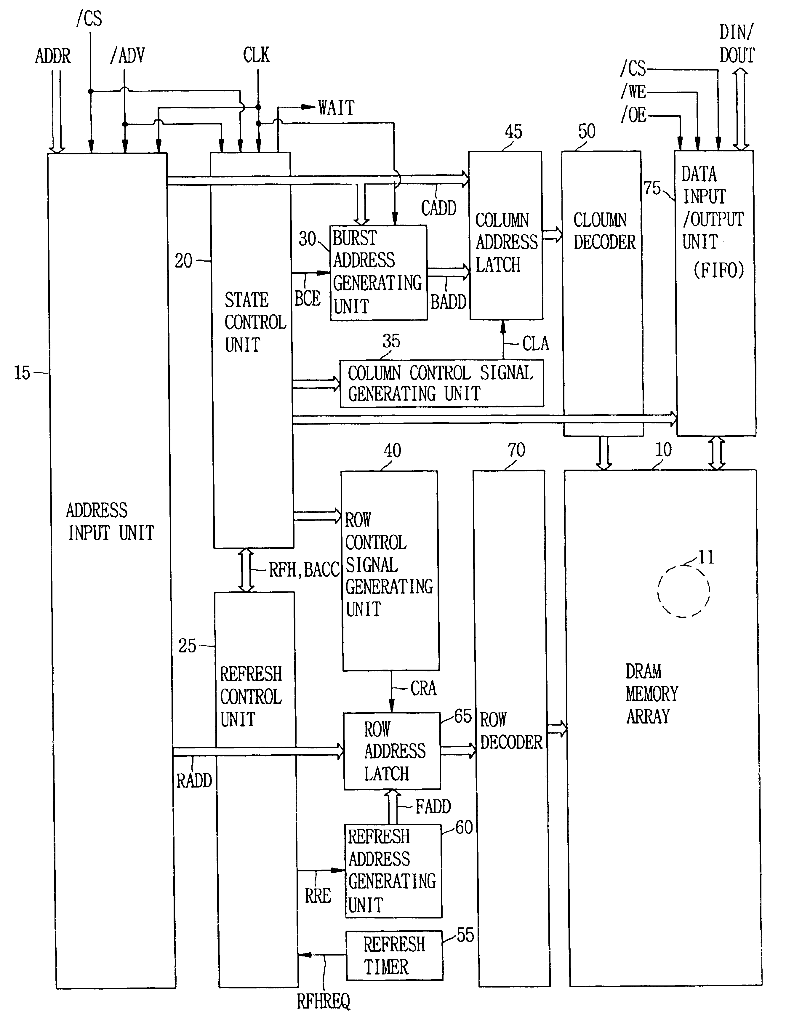
A synchronous SRAM-compatible memory according to the present invention employs DRAM cells and performs a refresh operation in its internal operation standpoint, but does not allocate an operational period to the refresh operation in its external operation standpoint. Additionally, the synchronous SRAM-compatible memory does not require an external control signal for controlling a refresh operation, and can be operated as does a general synchronous SRAM in its external operation standpoint.

The operations of the synchronous SRAM-compatible memory of the present invention are described in brief below.

The synchronous SRAM-compatible memory has a refresh state. In the refresh state, a refresh operation is performed for activating a selected word line, outputting data from all DRAM cells connected to the word line, am...


PUM


Abstract

The synchronous SRAM-compatible memory includes a DRAM array, a data input / output unit, an address input unit, a burst address generating unit, a state control unit, a refresh timer, and a refresh control unit. The data input / output unit controls input and output of data. The address input unit inputs a row address and a column address. The burst address generating unit generates a sequentially varying burst address. The state control unit generates a burst enable signal that enables the burst address generating unit, controls the data input / output unit, and generates a wait indication signal while an access operation of a previous frame is performed with respect to the memory array. The refresh timer generates a refresh request signal activated at regular intervals. The refresh control unit controls the refresh operation with respect to the DRAM array in response to the refresh request signal.

Description

BACKGROUND OF THE INVENTION1. Field of the InventionThe present invention relates generally to semiconductor memory devices, and more particularly to a memory device compatible with a synchronous static random access memory (SRAM) and a method of driving the same, in which the synchronous SRAM-compatible memory has dynamic random access memory cells and synchronizes with an external clock signal.2. Description of the Related ArtAs well known to those skilled in the art, a Random Access Memory (RAM), a type of semiconductor memory device, is generally classified into two types of memories, Static RAM (SRAM) and Dynamic RAM (DRAM). A general RAM includes a memory array composed of a plurality of unit memory cells arranged in a matrix form defined by rows and columns, and peripheral circuits adapted to control the input / output of data to / from the unit memory cells. Each of the unit memory cells in an SRAM stores one bit of data and has four transistors that form a latch structure and t...

Claims


Application Information

Patent Timeline
Patent Type & Authority Patents(United States)
IPC IPC(8): G11C7/10G11C11/406G11C11/401
CPCG11C7/1027G11C11/40615G11C11/406G11C7/1072G11C11/401
Inventor LEE, SUN HYOUNGYOO, IN SUNSHIN, DONG WOO
Owner MOSAID TECH
Features
  • R&D
  • Intellectual Property
  • Life Sciences
  • Materials
  • Tech Scout
  • Unparalleled Data Quality
  • Higher Quality Content
  • 60% Fewer Hallucinations
Learn More