Heat sink for a planar waveguide substrate

a planar waveguide and heat sink technology, applied in the direction of optical waveguide light guides, instruments, optics, etc., can solve the problems of insufficient heat dissipation, relatively large amount of heat generated in active regions of optical devices, and insufficient heat dissipation, etc., to achieve greater thermal conductivity

Inactive Publication Date: 2005-01-25
HOYA USA
View PDF2 Cites 12 Cited by
  • Summary
  • Abstract
  • Description
  • Claims
  • Application Information

AI Technical Summary

Benefits of technology

A substrate includes a recessed area or pit formed on the substrate surface, and heat sink material substantially filling the recessed area to form a heat sink. The heat sink material has thermal conductivity greater than that of the substrate. The heat sink may have a substantially flat surface substantially flush with the surface of the substrate. Polishing may be employed for forming substantially flush substrate and heat sink surfaces. The substrate may further include a planar optical waveguide formed on the substrate and positioned so as to establish optical coupling with an optical device mounted on the substrate in thermal contact with the heat sink. The substrate may further include an electrical contact layer formed on the substrate and positioned so as to establish electrical continuity with an optical device mounted on the substrate in thermal contact with the heat sink. The electrical contact may be positioned on the surface of the heat sink and also provide thermal contact, and solder may be employed for enhancing and securing electrical continuity and / or thermal contact with the device. The substrate may further include a low-index optical buffer layer formed on its surface; the surface of the optical buffer layer may be substantially flush with the heat sink. Materials for the substrate, buffer layer, and heat sink may include (but are not limited to): silicon, silica, and diamond, respectively.

Problems solved by technology

However, in certain instances the thermal conductivity of a silicon planar waveguide substrate may not be adequate for dissipating heat generated by devices and / or components on the substrate.
In many active devices, relatively large amounts of heat may be generated in active regions of the optical device, particularly if relatively large drive currents are required.
The small area for heat dissipation and the moderate thermal conductivity of the silicon substrate may therefore result in inadequate heat dissipation and potential overheating of the device.

Method used


Image

  • Heat sink for a planar waveguide substrate
  • Heat sink for a planar waveguide substrate
  • Heat sink for a planar waveguide substrate

Examples


Embodiment Construction

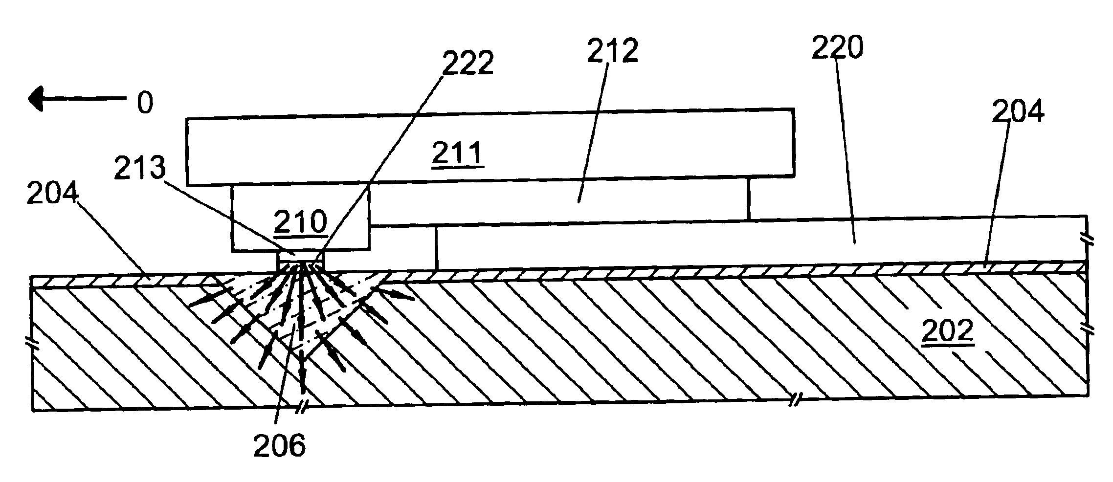
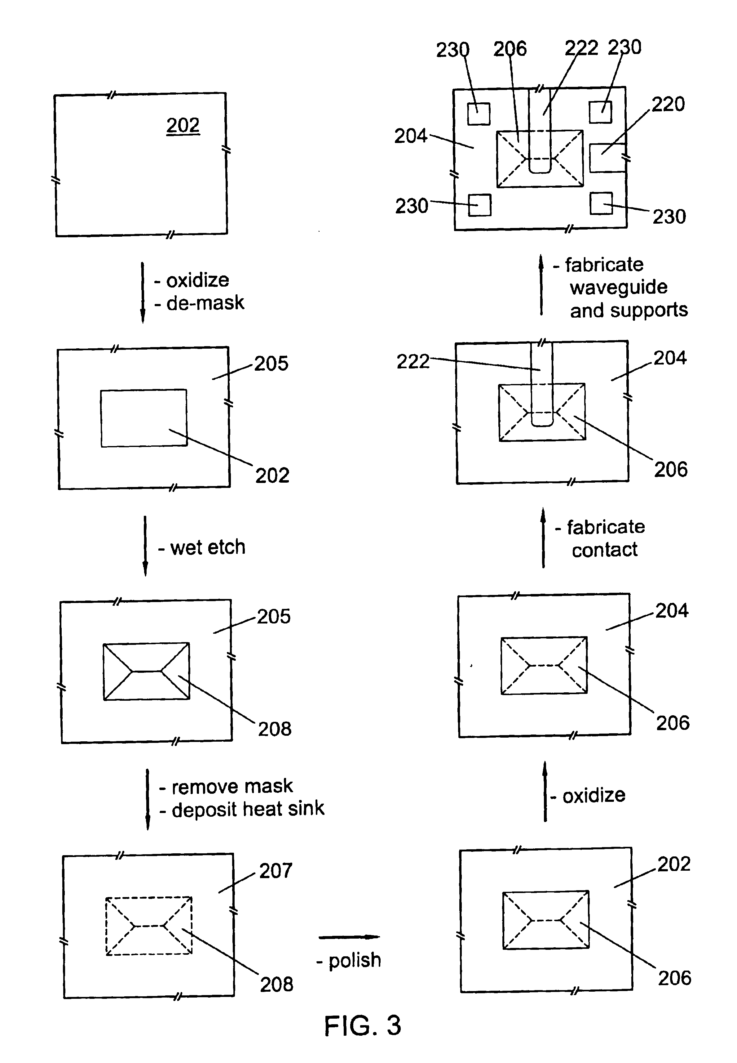
FIG. 2 shows an optical device mounted on a planar waveguide substrate with a heat sink according to the present invention. A silicon substrate 202 is provided with an optical buffer layer 204 and a heat sink 206. A planar waveguide 220 is formed on substrate 202 (with optical buffer layer 204 therebetween). An electrical contact 222 (typically Ti—Pt—Au several hundred nm thick; other suitable materials or material combinations may be equivalently employed) is formed on substrate 202 over portions of the buffer layer 204 and the heat sink 206. Heat sink 206 comprises material of greater thermal conductivity than substrate 202. An optical device 210 (on a device substrate 211 and including an external-transfer waveguide 212 in this example) is mounted on the planar waveguide substrate 202 (at least partially over heat sink 206) so as to establish electrical continuity with contact 222 (through device contact 213, typically Ti—Pt—Au; other materials or material combinations may be equ...


PUM

PropertyMeasurementUnit
thickaaaaaaaaaa
thermal conductivityaaaaaaaaaa
electrical continuityaaaaaaaaaa

Abstract

A recessed area formed on a substrate surface is filled with heat sink material to form a heat sink. The heat sink material has thermal conductivity greater than that of the substrate. The heat sink may have a substantially flat surface substantially flush with the substrate surface. The substrate may further include: a planar optical waveguide formed thereon positioned for optical coupling with an optical device mounted on the substrate in thermal contact with the heat sink; and/or an electrical contact layer formed thereon positioned for establishing electrical continuity with an optical device mounted on the substrate in thermal contact with the heat sink. The electrical contact may also provide thermal contact between the device and heat sink. The substrate may further include a low-index optical buffer layer formed on its surface. Materials for the substrate, buffer layer, and heat sink may include silicon, silica, and diamond, respectively.

Description

BACKGROUNDThe field of the present invention relates to planar waveguide substrates. In particular, heat sinks are described herein for facilitating heat dissipation on such substrates.Planar optical waveguides are suitable for implementing a variety of optical devices for use in telecommunications and other fields. In addition to the planar waveguides, the planar waveguide substrate often also includes (by fabrication, formation, and / or mounting thereon): alignment / support structures for placement of optical devices on the substrate; V-grooves and / or other alignment / support structures for positioning of optical fibers and / or fiber-optic tapers on the substrate; compensators, gratings, and / or other optical devices on the substrate; electrical contacts and / or traces for enabling electronic access to active devices on the substrate; and / or other suitable components.Silicon is a common substrate material for implementing planar optical waveguides, for a variety of reasons discussed fur...

Claims


Application Information

Patent Timeline
Patent Type & Authority Patents(United States)
IPC IPC(8): G02B6/12G02B6/42
CPCG02B6/12G02B6/4201G02B6/42
Inventor BENZONI, ALBERT M.DOWNIE, MARK D.
Owner HOYA USA
Why Eureka
Try Eureka