Wide band cross point switch using MEMS technology

a cross-point switch and wide-band technology, applied in waveguide devices, instruments, contacts, etc., can solve the problems of becoming more difficult to provide one single, massive stage to interconnect all inputs and outputs, and achieve the effect of improving signal separation

Inactive Publication Date: 2005-02-01
RAYTHEON CO
View PDF2 Cites 45 Cited by
  • Summary
  • Abstract
  • Description
  • Claims
  • Application Information

AI Technical Summary

Benefits of technology

The 64 MEMS are arranged in a square 8 by 8 matrix, as well as their controls. High frequency inputs and outputs to be switched by the MEMS are placed on the periphery of the substrate to further enhance the separation of signals. Terminating resistors (50 ohms) are also placed near the periphery.

Problems solved by technology

Unfortunately, as the size of the N×M matrix grows, it becomes more difficult to provide one single, massive, stage to interconnect all inputs and outputs.
The limitation to the number of stages is that, unlike the single stage design, the switched signal has to traverse a plurality of crosspoints within the exchange.

Method used


Image

  • Wide band cross point switch using MEMS technology
  • Wide band cross point switch using MEMS technology
  • Wide band cross point switch using MEMS technology

Examples


Embodiment Construction

1. Introduction

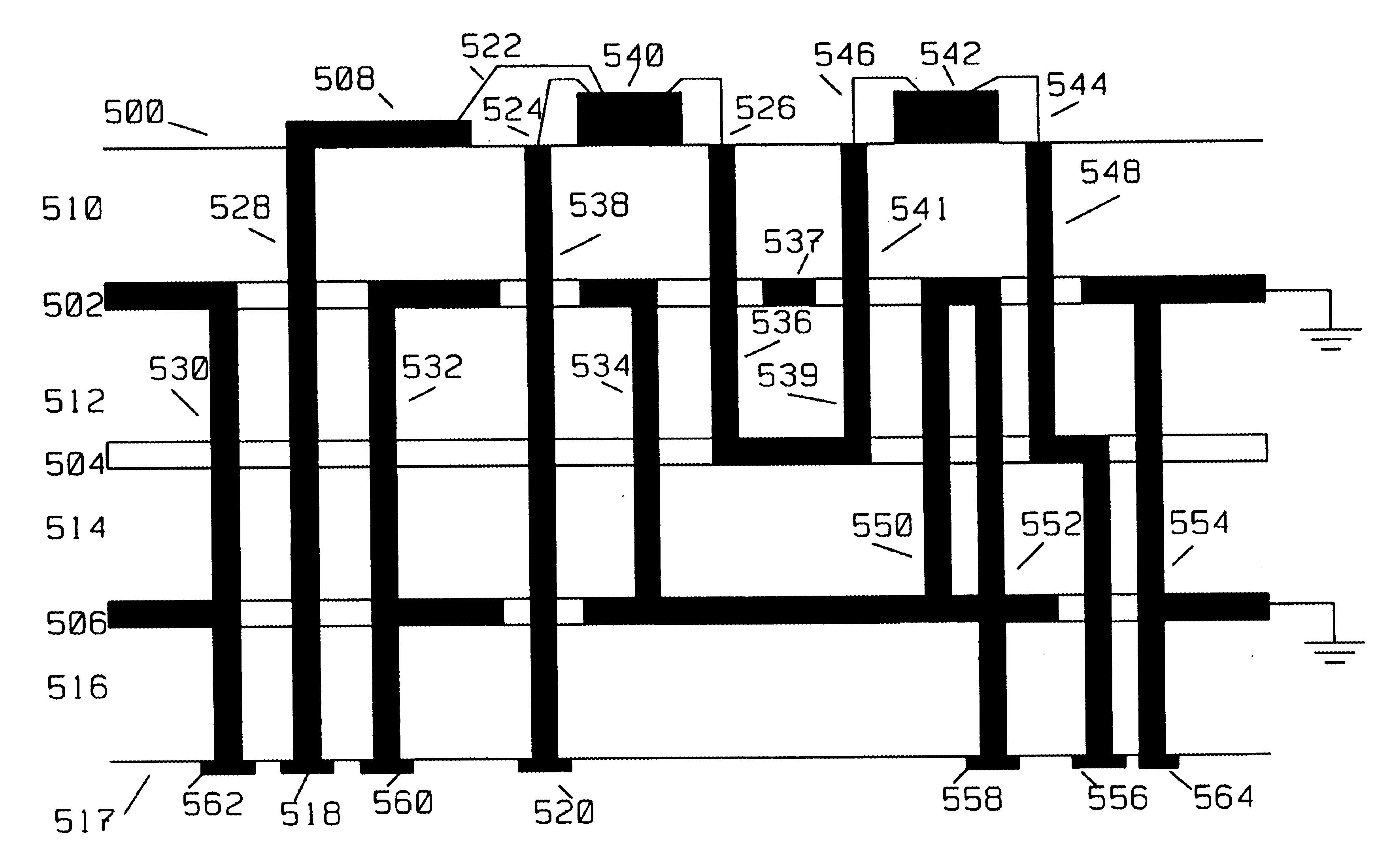
This invention introduces the notion of using MEMS structures on a common substrate to form, for example, an 8 by 8 switching matrix, as well as other switching matrix configurations. Special provisions are made to isolate the input from the output, thus insuring minimal signal leakage for OFF conditions across a MEMS structure.

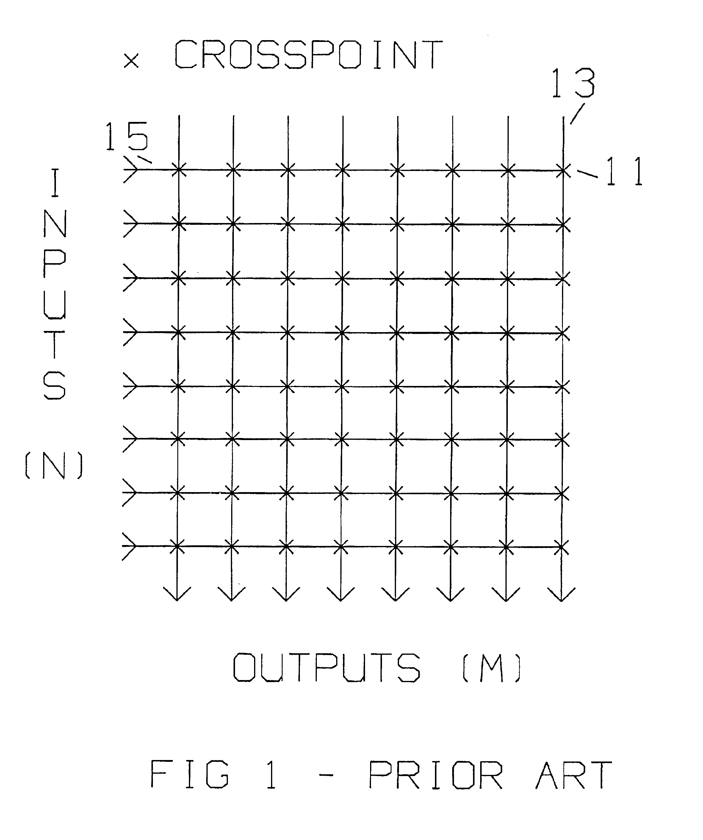
FIG. 1 shows a an 8 by 8 matrix of crosspoints of the prior art. Any of 8 inputs can be connected with any of 8 outputs. For example, input 15 is connected to output 13 using cross point switch 11. Because there are 64 cross point switches, this is a full availability, non-blocking switching matrix. Each of the 64 switches is closed or opened in accordance with a control signal applied to each switch. The control signals are not shown.

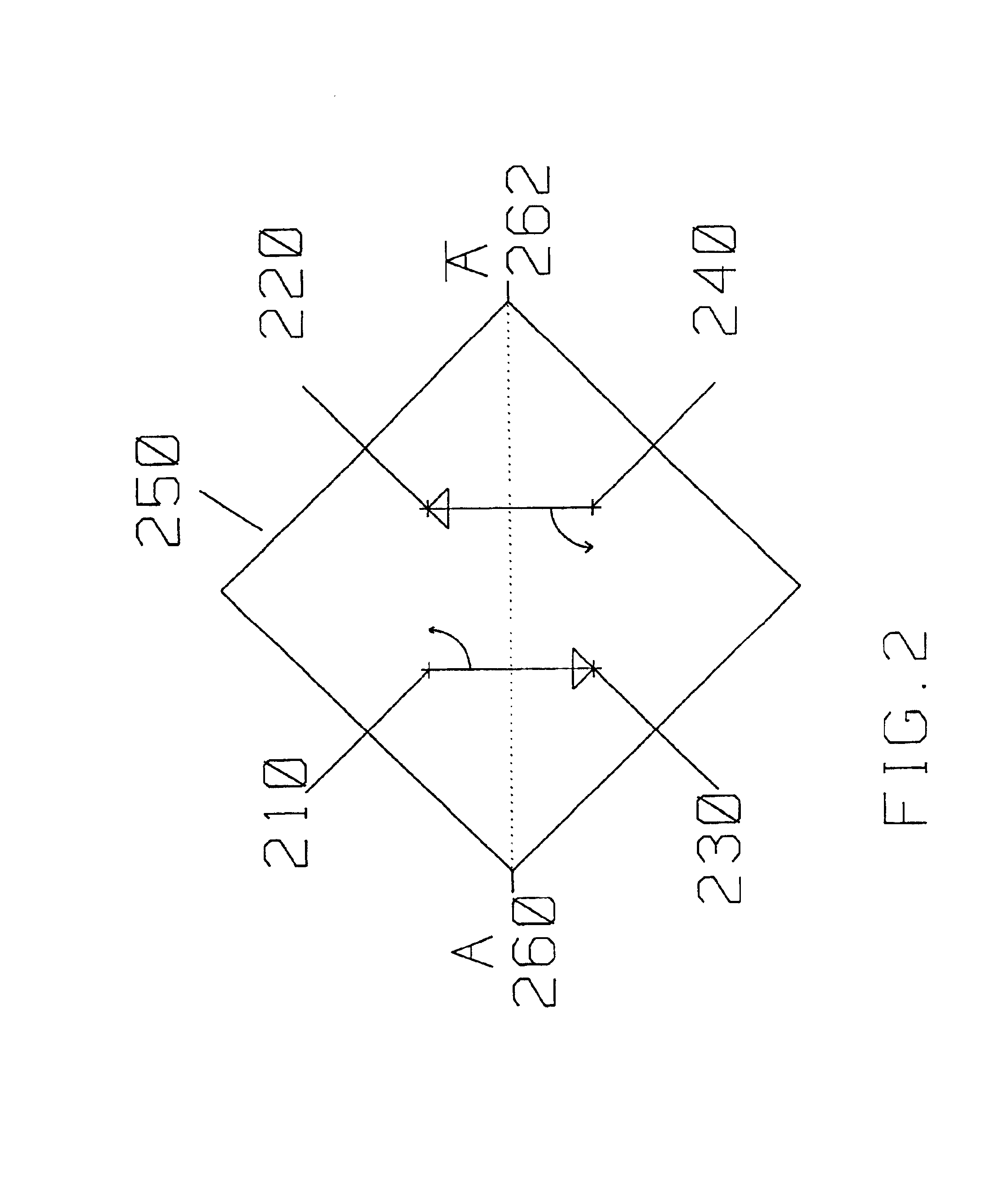
FIG. 2 shows the diagram of a typical MEMS structure 250, a building block of the present invention. In FIG. 2, a signal applied to terminal 210 can be switched to either terminal 230 or 220 upon a command applied...


PUM


Abstract

A multilayer switching assembly for switching high frequency signals has MEMS structures on a ceramic substrate having a top surface, a bottom surface and a plurality of insulating layers. The insulating layers are separated by a first conductor and a second conductor. The first conductor is connected to a ground potential. The second conductor is separated from the first conductor by one of the insulating layers. The second conductor presents a specific impedance (50 ohms) with respect to the first conductor to high frequency signals traveling on the second conductor.
64 MEMS structures are mounted on the top surface. Each MEMS has an input, an output, and a control. The input connected to the second conductor. The output is connected to a coplanar waveguide placed on the top surface. The control is connected to the bottom surface.
The input to each MEMS is electrically shielded from the output and from the control by a third conductor connected to the first (grounded) conductor. The third conductor traverses one or more of the insulating layers thereby acting as a shield and precluding the high frequency signals presented to the input from propagating to the output and to the control. The 64 MEMS are arranged in a square 8 by 8 matrix, as well as their controls. High frequency inputs and outputs to be switched by the MEMS are placed on the periphery of the substrate to further enhance the separation of signals. Terminating resistors (50 ohms) are also placed near the periphery.

Description

BACKGROUND OF THE INVENTION1. Field of inventionThis invention relates to the field of telephony, particularly forming a cross point switch using Microlectromechanical systems (MEMS) structures mounted on a ceramic substrate.2. Description of the Related ArtOne aspect of the art of telephony involves interconnecting any of a plurality of inputs, N, to any of a plurality of outputs M. It is desired to connect an input signal, part of N, carried on an incoming line, to an output, part of M, carried on an outgoing going line. This function is generally performed by an N×M matrix of crosspoints capable of interconnecting any member of N to any member of M. Such a structure of M×N crosspoints is a coordinate switch, that is, a rectangular array of crosspoints in which one side of the crosspoints is multiplied in rows and the other side in columns. A crosspoint is ideally a two state switching device having low transmission impedance in one state and very high in the other, as defined by ...

Claims


Application Information

Patent Timeline
Patent Type & Authority Patents(United States)
IPC IPC(8): H01H67/22H01H67/00H01P1/10H01P1/12H01H1/00
CPCH01H67/22H01P1/127H01H1/0036H01L2224/48095H01L2224/48227H01L2924/15192H01L2224/49109H01L2924/00014H01L2924/30111H01L2924/00
Inventor ALLISON, ROBERT C.LEE, JAR J.
Owner RAYTHEON CO
Why Eureka
Try Eureka