Semiconductor crystal film and method for preparation thereof

a technology of semiconductor devices and crystal films, applied in the direction of semiconductor devices, electrical devices, transistors, etc., can solve the problems of difficult dramatic improvement of device performance, limited optimal performance of resultant semiconductor devices, and many technical problems to be overcome. , to achieve the effect of convenient fabrication

Inactive Publication Date: 2005-02-08
PANASONIC CORP
View PDF21 Cites 102 Cited by
  • Summary
  • Abstract
  • Description
  • Claims
  • Application Information

AI Technical Summary

Benefits of technology

[0017]Each of the semiconductor layers in the multi-layer film may be thinner than the thickness at which discrete quantum levels arise in the layer. Then, the multi-layer film obtains a function as a single SiGeC layer easily.
[0026]Each of the semiconductor layers in the multi-layer film may be thinner than the thickness at which discrete quantum levels arise in the layer. Then, a semiconductor device that uses the multi-layer film having a function as a single SiGeC layer for its active region is obtained easily.
[0032]According to this method, a semiconductor crystal film that is a multi-layer film having the above-described function is easily produced.
[0037]According to this method, a semiconductor device having the semiconductor crystal film, which is the multi-layer film with the above-function, as an active region is easily fabricated.

Problems solved by technology

In order to pursue further performance-improvements, however, there exist many problems to be technically overcome other than semiconductor device scaling-down.
For example, even if the semiconductor elements have been further downsized, the optimal performance of the resultant semiconductor devices is restricted by the physical properties (e.g., mobility) of the base material, i.e., Si.
In other words, as long as a Si crystal is employed as the material, dramatical improvement in device performance will be problematic.
However, because of the unique properties of C to be described below, it is more difficult to produce a high-quality Si1-x-yGexCy crystal than to produce a Si1-xGex crystal.
Thus, producing a Si1-x-yGexCy crystal containing C at a high mole fraction (atm. percent order) becomes difficult under a thermal equilibrium condition during, for example, a fusion process.
Next, C atoms have a property of being easily incorporated into the lattice at an interstitial site as well as a substitutional site of the crystal, and thus the C atoms are likely to make the crystallinity worse.
Recently, the CVD method has been mainly used because the MBE method is inadequate for mass production.

Method used


Image

  • Semiconductor crystal film and method for preparation thereof
  • Semiconductor crystal film and method for preparation thereof
  • Semiconductor crystal film and method for preparation thereof

Examples


second embodiment

o the present invention.

[0047]FIG. 7 is a cross-sectional view schematically showing a structure of an npn heterojunction bipolar transistor (HBT) according to a third embodiment of the present invention.

[0048]FIG. 8 is a cross-sectional view showing a structure of the emitter-base-collector junction shown in FIG. 7 under magnification.

[0049]FIG. 9 is an energy band diagram schematically illustrating a band structure in cross-section through an emitter layer, a base layer and a collector layer when no bias is applied.

[0050]FIG. 10 is a cross-sectional view showing a structure of a heterojunction CMIS device (HCMIS device) utilizing a multi-layer film serving as a SiGeC layer for a p-channel, according to a fourth embodiment of the present invention.

[0051]FIG. 11 is a diagram conceptually showing a band state in a structure where a silicon layer, the multi-layer film and a silicon layer are stacked in the HCMIS device of the fourth embodiment.

BEST MODE FOR CARRYING OUT THE INVENTION

embodiment 1

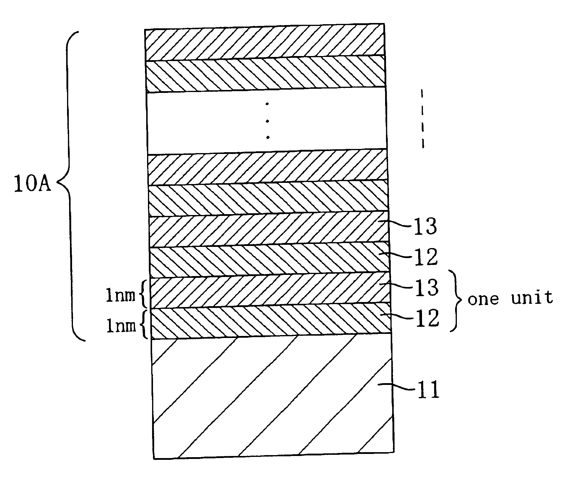
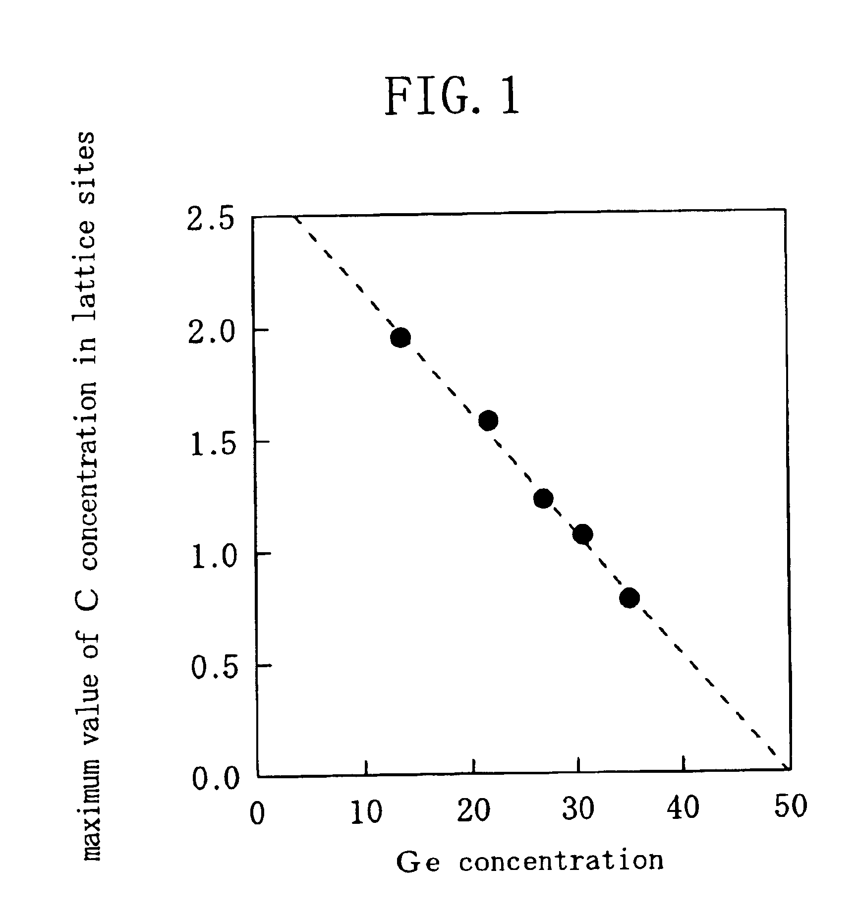
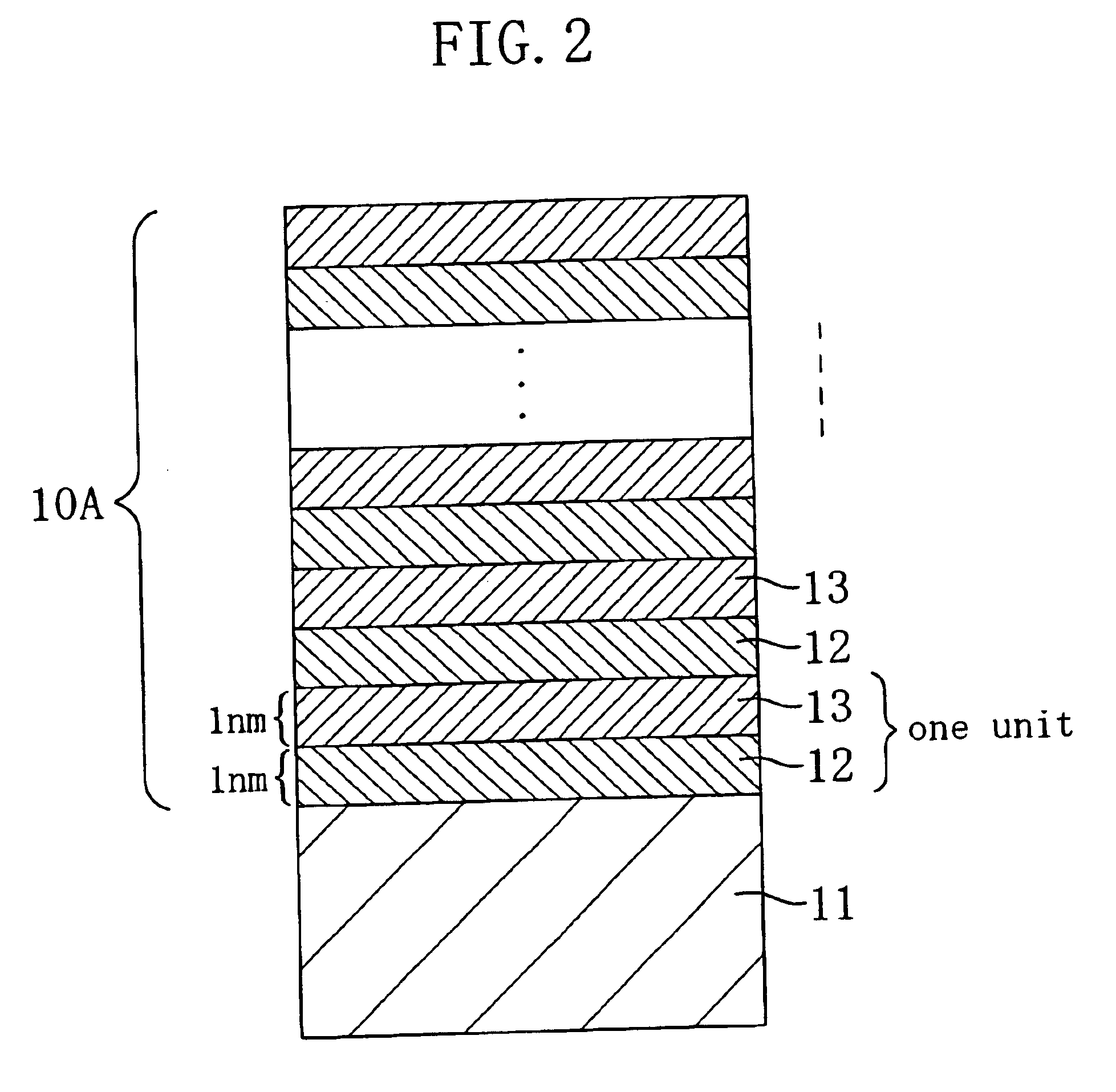
[0052]FIG. 2 is a cross-sectional view schematically showing a structure of a multi-layer film (a semiconductor crystal film) according to a first embodiment of the present invention. In this embodiment, a Si0.2Ge0.8 layer 12 with a thickness of about 1 nm having a larger lattice constant than Si crystal and a Si0.785Ge0.2C0.015 layer 13 with a thickness of about 1 nm are alternately deposited on a Si substrate 11 a plurality of times (50 cycles in this embodiment), thereby forming a multi-layer film 10A serving as a SiGeC layer with a thickness of about 100 nm. The multi-layer film 10A of this embodiment is considered to have a superlattice structure with little discrete quantum levels. Hereinafter, it will be described how the multi-layer film 10A is formed. FIGS. 3(a) through 3(e) are cross-sectional views showing respective process steps for producing a semiconductor crystal film according to the first embodiment.

[0053]In this embodiment, the Si0.2Ge0.8 layer 12 and the Si0.785G...

embodiment 2

[0071]In the first embodiment, the inventive multi-layer film, which is obtained by alternate epitaxial growths of two crystal films having two mutually different compositions, and the method for producing the film have been described. In this embodiment, another inventive multi-layer film that is obtained by alternate epitaxial growths of three crystal layers having mutually different compositions will be described.

[0072]FIG. 6 is a cross-sectional view schematically showing a structure of a multi-layer film (a semiconductor crystal film) according to a second embodiment of the present invention. In this embodiment, a Si0.2Ge0.8 layer 12 with a thickness of about 1 nm having a larger lattice constant than Si crystal and a Si0.785Ge0.2C0.015 layer 13 with a thickness of about 1 nm, and a Si0.832Ge0.15C0.018 layer 14 with a thickness of about 1 nm are alternately deposited on a Si substrate 11 a plurality of times (33 cycles in this embodiment), thereby forming a multi-layer film 10C...


PUM


Abstract

A multi-layer film 10 is formed by stacking a Si1-x1-y1Gex1Cy1 layer (0≦x1<1 and 0<y1<1) having a small Ge mole fraction, e.g., a Si0.785Ge0.2C0.015 layer 13, and a Si1-x2-y2Gex2Cy2 layer (0<x2≦1 and 0≦y2<1) (where x1<x2 and y1>y2) having a high Ge mole fraction, e.g., a Si0.2Ge0.8 layer 12. In this manner, the range in which the multi-layer film serves as a SiGeC layer with C atoms incorporated into lattice sites extends to high degrees in which a Ge mole fraction is high.

Description

TECHNICAL FIELD[0002]The present invention relates to semiconductor crystal films that contain Si, C and Ge and have high crystallinity, to methods for producing the films, to semiconductor devices including the semiconductor crystal films, and to methods for fabricating the devices.BACKGROUND ART[0003]Recently, semiconductor devices using Si crystals have attained improved multifunctionality and high-speed capability in turns. This attainment is largely attributable to scaling-down of transistors and other semiconductor elements. To continue to improve semiconductor-device performance in the future, further scaling-down of semiconductor elements is necessary. In order to pursue further performance-improvements, however, there exist many problems to be technically overcome other than semiconductor device scaling-down.[0004]For example, even if the semiconductor elements have been further downsized, the optimal performance of the resultant semiconductor devices is restricted by the p...

Claims


Application Information

Patent Timeline
Patent Type & Authority Patents(United States)
IPC IPC(8): H01L21/02H01L29/02H01L21/205H01L29/66H01L29/15H01L29/737H01L29/80H01L29/24
CPCH01L29/155H01L29/7378H01L29/802H01L21/02507H01L21/02381H01L21/02661H01L21/0245H01L21/02505H01L21/02529H01L21/02532H01L21/0262H01L21/02447H01L29/1608
Inventor KANZAWA, YOSHIHIKOSAITOH, TOHRUNOZAWA, KATSUYAKUBO, MINORUHARA, YOSHIHIROTAKAGI, TAKESHIKAWASHIMA, TAKAHIRO
Owner PANASONIC CORP
Why Eureka
Try Eureka