Electrical interconnect structures for integrated circuits and methods of manufacturing the same

a technology of electrical interconnection and integrated circuit, which is applied in the direction of manufacturing tools, contact member manufacturing, and welding apparatus, etc., and can solve the problem of recognizing that cu(n) is also relatively unstabl

Inactive Publication Date: 2007-11-13
KULICKE & SOFFA IND INC
View PDF12 Cites 18 Cited by
  • Summary
  • Abstract
  • Description
  • Claims
  • Application Information

AI Technical Summary

Benefits of technology

[0012]Applicants have discovered a solution which overcomes the problems noted above and which provides other beneficial and desirable results. More particularly, the present invention relates to interconnect structures and methods which utilize a bonding surface comprising copper nitride. Applicants have discovered that interconnect structures which include a bonding surface comprising copper nitride can be highly effective at preventing oxidation and / or other unwanted corrosion of the underlying conductive material while at the same time providing the basis for a high conductivity bond. Furthermore, applicants' invention provides the advantage of simplifying and / or reducing the cost of the manufacturing process. These benefits derive, at least in part, from applicants' recognition and discovery that copper nitride is capable of providing in such structures a relatively non-conductive, corrosion-resistant bonding surface while at the same time being readily transformed into a conductive layer at or just prior to the time of bonding. According to certain embodiments of the method aspects of the present invention, an interconnect bonding structure is formed by providing a conductive base material having a relatively non-conductive, corrosion-resistant bonding surface comprising Cu(N), forming an electrically conductive bond in the region of said bonding surface; and prior to or substantially simultaneously with said bond forming step, decomposing a sufficient amount of the Cu(N) in said bonding surface to produce a substantial increase in the conductivity of the layer containing the Cu(N) and thereby forming a relatively conductive bonding surface. Preferably the decomposing step causes a change in conductivity sufficient to produce a commercially acceptable electrical connection.
[0016]Further, it is believed that copper-nitrogen mixtures, even with only a small amount of nitrogen included, are effective at reducing electrical conductivity and increasing corrosion resistance. It is also believed that such mixtures are also readily decomposed to copper and nitrogen and thus are capable, under the appropriate conditions, of being converted to a highly conductive layer just prior to or at about the time the bond is formed. Accordingly, the term “Cu(N)” is used herein to mean and identify all phases and compounds consisting essentially of nitrogen and copper. The notation “Cu(N)” as used herein thus indicates that some or all of nitrogen may be bound (covalently and / or ionically) to the copper, such as in Cu3N, but is not limited to this compound. Thus, the notation “Cu(N)’ also covers the possible, but less common, stoichiometry Cu4N and other effective stoichiometries and / or combinations of copper and nitrogen.
[0017]The non-conductive nature of the Cu(N) and the methods of forming it present another advantage in that no mask is required to form it on a semiconductor device. In some embodiments, the Cu(N) may be applied over the entire device or over large potions of the device without a mask without forming electrical shorts between bond pads because Cu(N) is essentially non-conducting. In other embodiments, the Cu(N) may be formed by converting a surface layer of existing copper interconnect elements to Cu(N). In this manner, no Cu(N) is formed between separate copper interconnect elements, such as bond pads.

Problems solved by technology

However, applicants have come to appreciate that Cu(N)is also relatively unstable, particularly under the conditions which are frequently encountered as a surface is prepared for and / or exposed to bonding operations.

Method used


Image

  • Electrical interconnect structures for integrated circuits and methods of manufacturing the same
  • Electrical interconnect structures for integrated circuits and methods of manufacturing the same
  • Electrical interconnect structures for integrated circuits and methods of manufacturing the same

Examples


example 1

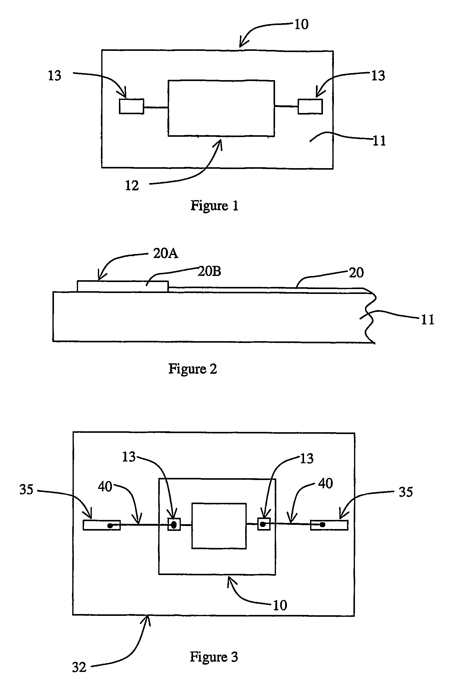
[0037]A silicon die comprising a substrate and a conductive copper layer, of the general type illustrated in FIG. 2, is provided. The conductive copper layer is 10,000 Angstroms and forms the base for a bond pad on the die. A protective surface is formed on the bond pad by first pre-treating the bonding surface with a gaseous composition consisting of about 95 mole % nitrogen (N2) and 5 mole % of hydrogen (H2). The surface is exposed to this first pre-treating gas at a temperature of about 400° C. for about nine (9) hours to produce a bonding surface that is substantially free of copper oxide. The bonding surface is then exposed to a second pre-treating step by exposure to a gaseous composition consisting essentially of oxygen (O2) at a temperature of about 200° C. for about five (5) minutes to produce a copper oxide layer with a well-controlled thickness. The oxide layer is then treated with anhydrous ammonia for 5 hours at about 275° C. to produce a substantially non-conductive su...

example 2

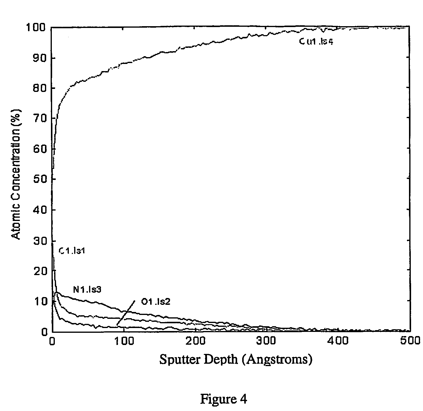
[0038]Copper nitride is deposited onto a quarter of an 8-inch silicon wafer with a uniform 1 micron thick copper coating by radio-frequency sputtering of a copper target in an atmosphere of approximately 4 mtorr nitrogen. A 200 Angstrom deposit is produced at a sputtering rate of approximately 33 Angstrom per minute. During the process, the wafer is heated to 100° C. FIG. 5 shows a Auger depth profile of the elemental composition. The Auger data clearly indicates a copper nitride coating with a thickness of about 200 Angstrom. The silicon and oxygen are most likely contaminants present on the wafer before the experiment.

example 3

[0039]Copper nitride is deposited by a vacuum deposition technique as follows. Helium gas at a pressure of approximately 1 atmosphere pressure is passed through a nozzle situated approximately 10 cm above a copper-coated silicon wafer in a vacuum chamber. The substrate is heated to approximately 120° C. An electric discharge between an anode and a copper hollow cathode sputtering target inside the nozzle introduce copper atoms and ions into the helium. Nitrogen gas is introduced below the nozzle to produce a background pressure of approximately 30 mtorr of nitrogen. The interaction of the copper atoms or ions with the nitrogen causes the deposition of copper nitride on the surface. FIG. 6 shows an Auger elemental depth profile for the sample produced in this experiment. The depth profile demonstrates the formation of a surface layer of copper nitride with a thickness of about 50 Angstroms on the copper-coated wafer. The oxygen seen at a greater depth is the copper oxide that existed...


PUM

PropertyMeasurementUnit
temperaturesaaaaaaaaaa
temperatureaaaaaaaaaa

Abstract

Disclosed are interconnect structures and methods which utilize a bonding surface comprising copper nitride. The interconnect structures include a bonding surface comprising copper nitride which is effective at preventing oxidation and / or other unwanted corrosion of the underlying conductive material while providing the basis for a high conductivity bond. The copper nitride bonding surface provides a relatively non-conductive, corrosion-resistant bonding surface while at the same time being readily transformed into a conductive layer at or just prior to the time of bonding.

Description

CROSS REFERENCE TO RELATED APPLICATIONS[0001]This application is the National Stage Filing of PCT Application No. PCT / US04 / 010861 filed on Apr. 9, 2004 which, in turn, claims priority benefit under 35 U.S.C. Section 119(e) of U.S. Provisional Application No. U.S. 60 / 461,776 filed on Apr. 9, 2003. The contents of both applications are hereby incorporated by reference.FIELD OF THE INVENTION[0002]The present invention relates to the field of interconnect structures for integrated circuit packages and to methods of fabricating same, and more particularly to copper interconnect structures for electrically connecting two or more electronic components.BACKGROUND[0003]Interconnection technology is an important aspect of the fabrication of electronic components containing semiconductor devices. For example, in chip bonding, the back of a chip is mechanically attached to an appropriate medium, such as a ceramic substrate, a paddle of a metal lead frame or to a ball grid array (BGA). The upper...

Claims


Application Information

Patent Timeline
Patent Type & Authority Patents(United States)
IPC IPC(8): B32B37/00H01L21/60H01L21/603H01L21/607H01L23/485
CPCH01L24/81H01L24/85H01L24/05H01L24/45H01L2224/05599H01L2224/45144H01L2224/45147H01L2224/48H01L2224/49175H01L2224/81801H01L2224/85205H01L2224/85399H01L2924/01002H01L2924/01006H01L2924/01007H01L2924/01013H01L2924/01014H01L2924/01015H01L2924/01018H01L2924/01022H01L2924/01029H01L2924/0103H01L2924/01033H01L2924/0104H01L2924/01047H01L2924/0105H01L2924/01073H01L2924/01074H01L2924/01078H01L2924/01079H01L2924/01082H01L2924/014H01L2924/04941H01L2924/04953H01L2924/05042H01L2924/14H01L2924/19041H01L2924/19043H01L2924/3011H01L2924/3025H01L2924/00014H01L2924/01084H01L2924/12041H01L2924/10253H01L2224/05554H01L2224/04042Y10T29/49204H01L2224/78H01L2924/00H01L2224/45015H01L2924/15747H01L2924/15787H01L2224/45124H01L24/49H01L24/48H01L2224/85203H01L2924/20751H01L2924/20753H01L2924/00015
Inventor BEATSON, DAVID T.CLAUBERG, HORSTDURY, KENNETH K.
Owner KULICKE & SOFFA IND INC
Why Eureka
Try Eureka