Interconnect apparatus and methods

a technology of interconnection and components, applied in the direction of manufacturing tools, contact member manufacturing, welding apparatus, etc., can solve the problem of recognizing that cu(n) is also relatively unstabl

Inactive Publication Date: 2007-02-01
KULICKE & SOFFA IND INC
View PDF8 Cites 15 Cited by
  • Summary
  • Abstract
  • Description
  • Claims
  • Application Information

AI Technical Summary

Benefits of technology

[0016] The non-conductive nature of the Cu(N) and the methods of forming it present another advantage in that no mask is required to form it on a semiconductor device. In some embodiments, the Cu(N) may be applied over the entire device or over large potions of the device without a mask without forming electrical shorts between bond pads because Cu(N) is essentially non-conducting. In other embodiments, the Cu(N) may be formed by converting a surface layer of existing copper interconnect elements to Cu(N). In this manner, no Cu(N) is formed between separate copper interconnect elements, such as bond pads.

Problems solved by technology

However, applicants have come to appreciate that Cu(N)is also relatively unstable, particularly under the conditions which are frequently encountered as a surface is prepared for and / or exposed to bonding operations.

Method used


Image

  • Interconnect apparatus and methods
  • Interconnect apparatus and methods
  • Interconnect apparatus and methods

Examples


example 1

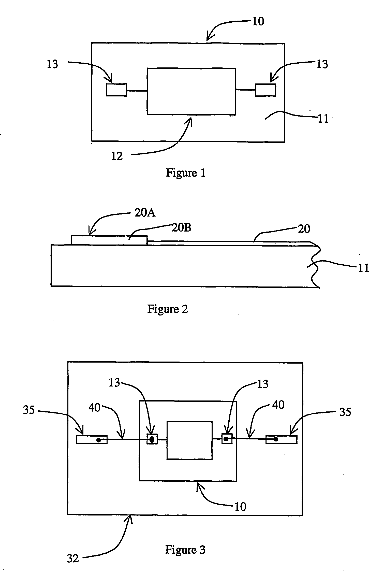
[0036] A silicon die comprising a substrate and a conductive copper layer, of the general type illustrated in FIG. 2, is provided. The conductive copper layer is 10,000 Angstroms and forms the base for a bond pad on the die. A protective surface is formed on the bond pad by first pre-treating the bonding surface with a gaseous composition consisting of about 95 mole % nitrogen (N2) and 5 mole % of hydrogen (H2). The surface is exposed to this first pre-treating gas at a temperature of about 400° C. for about nine (9) hours to produce a bonding surface that is substantially free of copper oxide. The bonding surface is then exposed to a second pre-treating step by exposure to a gaseous composition consisting essentially of oxygen (O2) at a temperature of about 200° C. for about five (5) minutes to produce a copper oxide layer with a well-controlled thickness. The oxide layer is then treated with anhydrous ammonia for 5 hours at about 275° C. to produce a substantially non-conductive s...

example 2

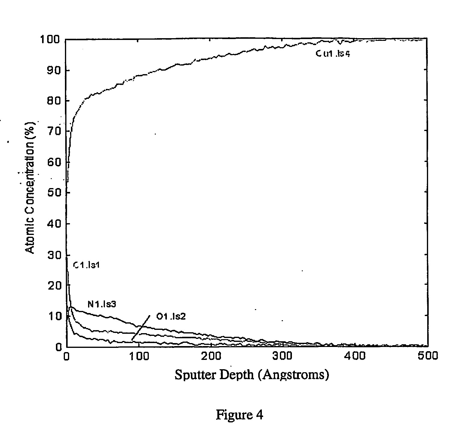
[0037] Copper nitride is deposited onto a quarter of an 8-inch silicon wafer with a uniform 1 micron thick copper coating by radio-frequency sputtering of a copper target in an atmosphere of approximately 4 mtorr nitrogen. A 200 Angstrom deposit is produced at a sputtering rate of approximately 33 Angstrom per minute. During the process, the wafer is heated to 100° C. FIG. 5 shows a Auger depth profile of the elemental composition. The Auger data clearly indicates a copper nitride coating with a thickness of about 200 Angstrom. The silicon and oxygen are most likely contaminants present on the wafer before the experiment.

example 3

[0038] Copper nitride is deposited by a vacuum deposition technique as follows. Helium gas at a pressure of approximately 1 atmosphere pressure is passed through a nozzle situated approximately 10 cm above a copper-coated silicon wafer in a vacuum chamber. The substrate is heated to approximately 120° C. An electric discharge between an anode and a copper hollow cathode sputtering target inside the nozzle introduce copper atoms and ions into the helium. Nitrogen gas is introduced below the nozzle to produce a background pressure of approximately 30 mtorr of nitrogen. The interaction of the copper atoms or ions with the nitrogen causes the deposition of copper nitride on the surface. FIG. 6 shows an Auger elemental depth profile for the sample produced in this experiment. The depth profile demonstrates the formation of a surface layer of copper nitride with a thickness of about 50 Angstroms on the copper-coated wafer. The oxygen seen at a greater depth is the copper oxide that existe...


PUM

PropertyMeasurementUnit
temperaturesaaaaaaaaaa
temperatureaaaaaaaaaa

Abstract

Disclosed are interconnect structures and methods which utilize a bonding surface comprising copper nitride. The interconnect structures include a bonding surface comprising copper nitride which is effective at preventing oxidation and/or other unwanted corrosion of the underlying conductive material while providing the basis for a high conductivity bond. The copper nitride bonding surface provides a relatively non-conductive, corrosion-resistant bonding surface while at the same time being readily transformed into a conductive layer at or just prior to the time of bonding.

Description

FIELD OF THE INVENTION [0001] The present invention relates to the field of interconnect structures for integrated circuit packages and to methods of fabricating same, and more particularly to copper interconnect structures for electrically connecting two or more electronic components. BACKGROUND [0002] Interconnection technology is an important aspect of the fabrication of electronic components containing semiconductor devices. For example, in chip bonding, the back of a chip is mechanically attached to an appropriate medium, such as a ceramic substrate, a paddle of a metal lead frame or to a ball grid array (BGA). The upper level of wiring for the chip normally includes bond pads which are electrically attached, via the necessary connections, to the underlying circuit. The chip commonly has a protective overcoat (PO) layer, generally referred to as passivation, with holes providing access to the bond pads. The bond pads on the circuit side of the chip are electrically connected to...

Claims


Application Information

Patent Timeline
Patent Type & Authority Applications(United States)
IPC IPC(8): H01L21/00H01L23/495H01L21/60H01L21/603H01L21/607H01L23/485
CPCH01L24/45H01L24/81H01L24/85H01L2224/05599H01L2224/45144H01L2224/45147H01L2224/48H01L2224/49175H01L2224/81801H01L2224/85205H01L2224/85399H01L2924/01002H01L2924/01006H01L2924/01007H01L2924/01013H01L2924/01014H01L2924/01015H01L2924/01018H01L2924/01022H01L2924/01029H01L2924/0103H01L2924/01033H01L2924/0104H01L2924/01047H01L2924/0105H01L2924/01073H01L2924/01074H01L2924/01078H01L2924/01079H01L2924/01082H01L2924/014H01L2924/04941H01L2924/04953H01L2924/05042H01L2924/14H01L2924/19041H01L2924/19043H01L2924/3011H01L2924/3025H01L24/05H01L2924/00014H01L2924/01084H01L2924/12041H01L2924/10253H01L2224/05554H01L2224/04042Y10T29/49204H01L2224/78H01L2924/00H01L2224/45015H01L2924/15747H01L2924/15787H01L2224/45124H01L24/49H01L24/48H01L2224/85203H01L2924/20751H01L2924/20753H01L2924/00015
Inventor BEATSON, DAVID T.CLAUDERG, HORSTDURY, KENNETH K.
Owner KULICKE & SOFFA IND INC
Why Eureka
Try Eureka