Embedded multilayer ceramic electronic component and method of manufacturing the same, and printed circuit board having embedded multilayer ceramic electronic component therein

a multi-layer ceramic electronic component and embedded technology, which is applied in the direction of fixed capacitor details, printed circuit non-printed electric components association, final product manufacturing, etc., can solve the problems of significant increase in manufacturing costs in the manufacturing process of printed circuit boards, defects in the adhesive surface between the board and the multi-layer ceramic electronic components, and insufficient space for mounting passive elements on printed circuit boards. achieve the effect of improving delamination and enhancing adhesive characteristics

Inactive Publication Date: 2014-06-05
SAMSUNG ELECTRO MECHANICS CO LTD
View PDF7 Cites 17 Cited by
  • Summary
  • Abstract
  • Description
  • Claims
  • Application Information

AI Technical Summary

Benefits of technology

[0012]An aspect of the present invention provides an embedded multilayer ceramic electronic component, capable of improving delamination between a multilayer ceramic electronic component and a board and thus enhancing adhesive characteristics thereof, by controlling surface roughness of a ceramic surface of the multilayer ceramic electronic component and surface roughness of the plating layer, a method of manufacturing the embedded multilayer ceramic electronic component, and a printed circuit board having the embedded multilayer ceramic electronic component therein.

Problems solved by technology

As electronic circuits are provided with higher levels of density and integration, space provided for mounting passive elements on a printed circuit board may be insufficient.
This laser process may significantly increase manufacturing costs in a printed circuit board manufacturing process.
In this case, defects in an adhesive surface between the board and the multilayer ceramic electronic component may occur due to differences in coefficients of thermal expansion (CTE) between the epoxy resin, the metal electrode, the ceramic material of the multilayer ceramic electronic component, and the like, or through thermal expansion of the board.
These defects may cause faults, such as delamination of the adhesive surface, during a reliability test.

Method used


Image

  • Embedded multilayer ceramic electronic component and method of manufacturing the same, and printed circuit board having embedded multilayer ceramic electronic component therein
  • Embedded multilayer ceramic electronic component and method of manufacturing the same, and printed circuit board having embedded multilayer ceramic electronic component therein
  • Embedded multilayer ceramic electronic component and method of manufacturing the same, and printed circuit board having embedded multilayer ceramic electronic component therein

Examples


##ventive example 1

INVENTIVE EXAMPLE 1

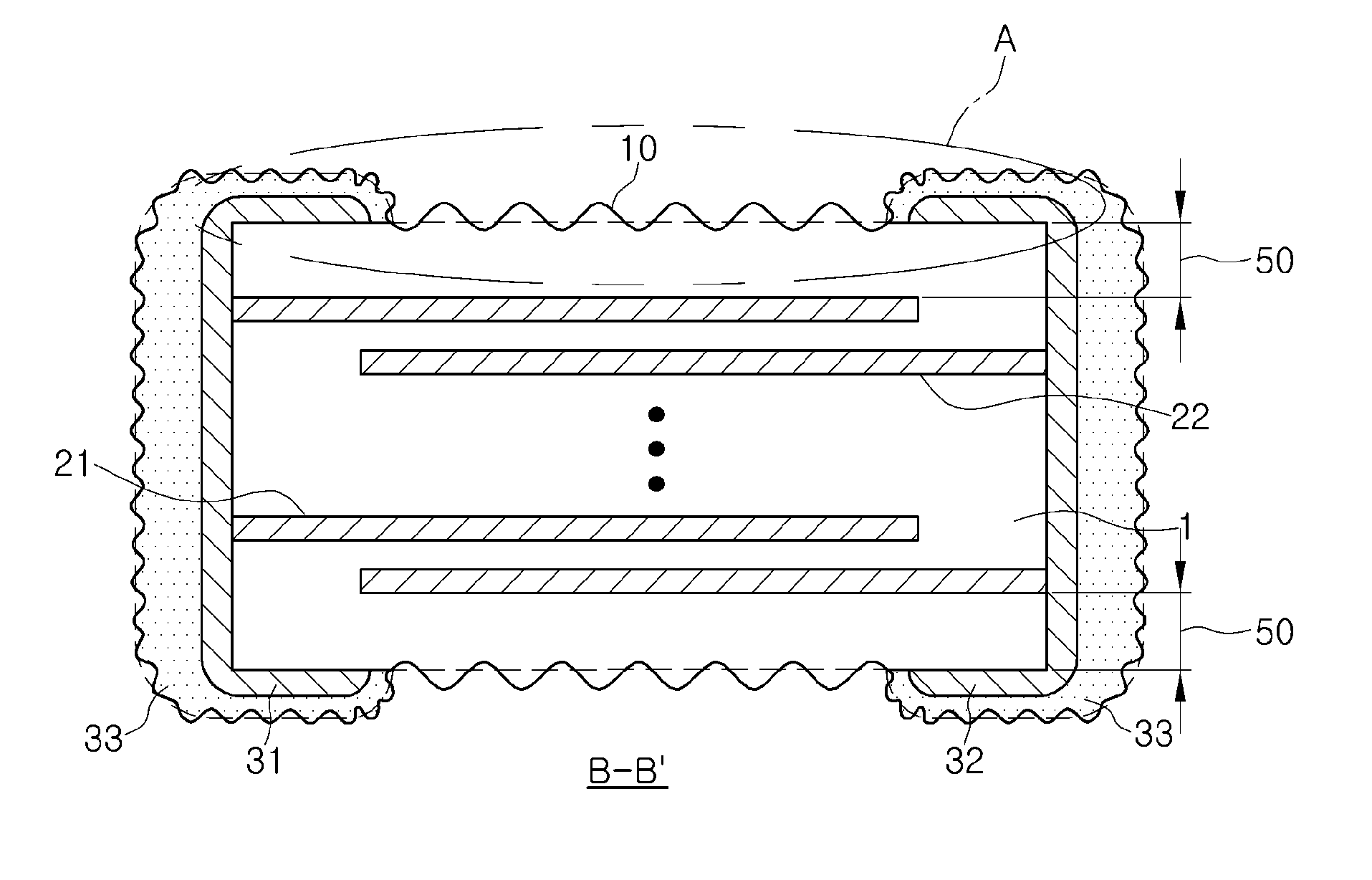
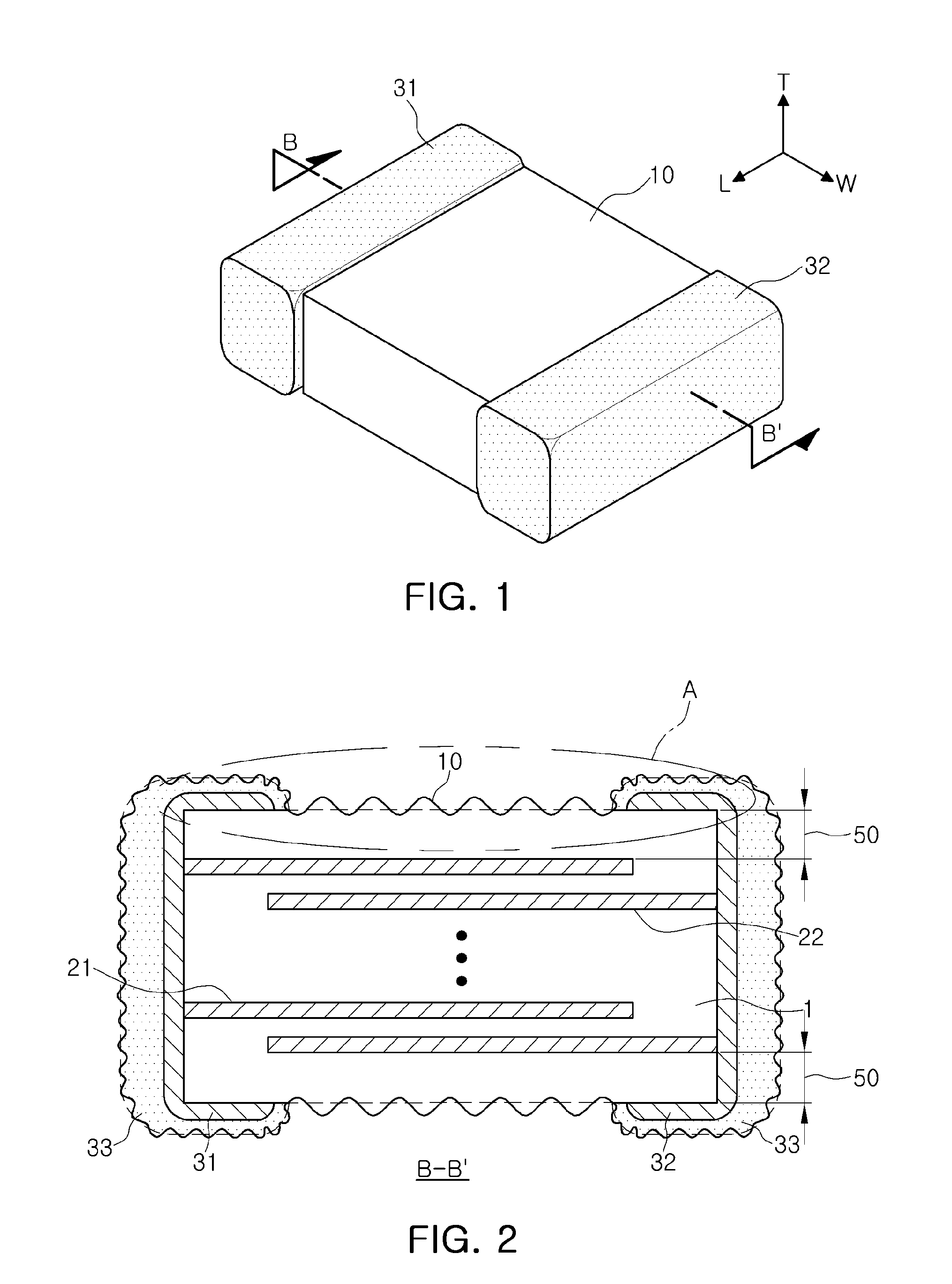
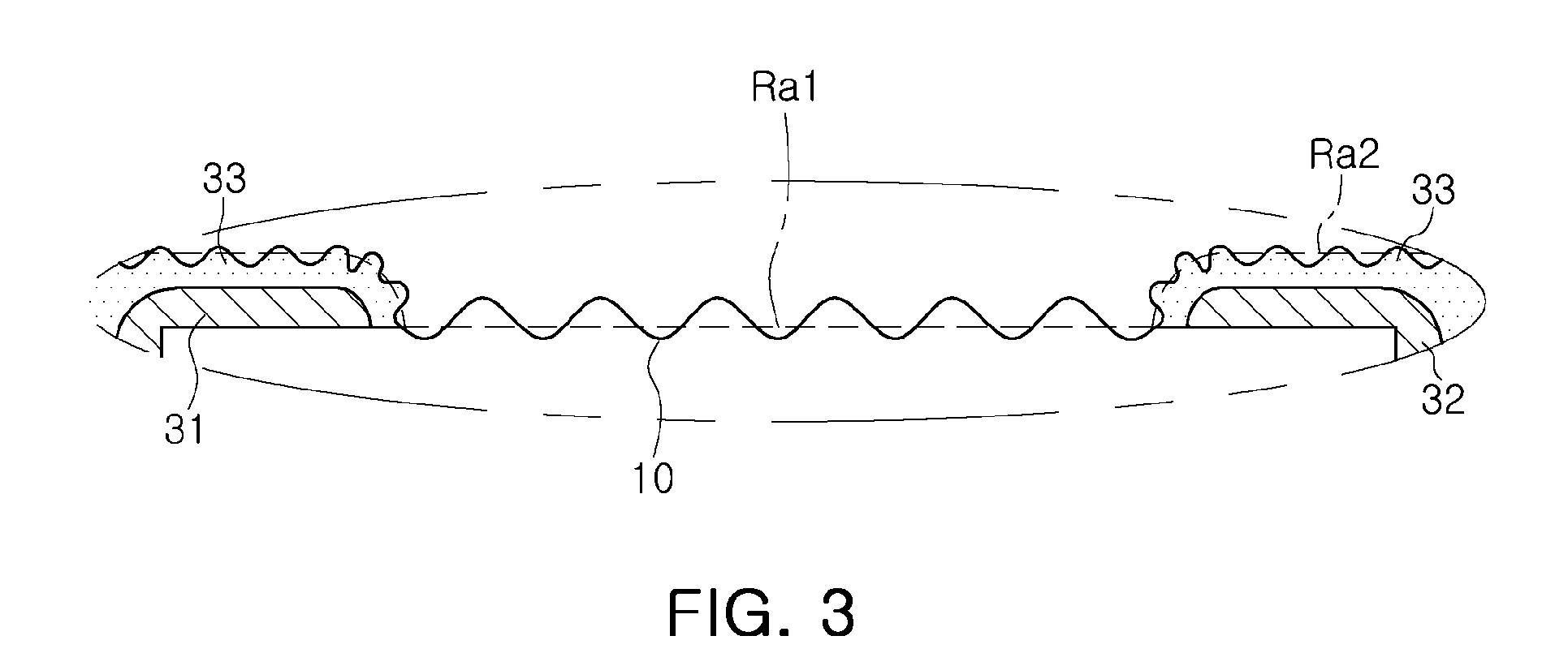
[0081]In order to confirm the frequency of delamination of the adhesive surface depending on the surface roughness of the embedded multilayer ceramic electronic component according to the embodiment of the invention, a board having a multilayer ceramic electronic component embedded therein is allowed to be left for 30 minutes and then the frequency of delamination was measured and investigated at a temperature of 85° C. and relative humidity of 85%, which corresponds to a general severe condition of a chip component for a mobile phone mother board (Severe Condition 1) and at a temperature of 125° C. and relative humidity of 85%, which corresponds to a severe condition according to higher functions of an application processor (AP) (Severe Condition 2) while the center line average roughness of the ceramic body 10 (Ra1) and the center line average roughness of the plating layer 33 (Ra2) were varied according to the thickness of the plating layer 33.

[0082]Experimenta...


PUM

PropertyMeasurementUnit
surface roughnessaaaaaaaaaa

Abstract

There is provided an embedded multilayer ceramic electronic component, including: a ceramic body including dielectric layers; first and second internal electrodes facing each other with the dielectric layers interposed therebetween; a first external electrode and a second external electrode formed on external surfaces of the ceramic body, the first external electrode being electrically connected to the first internal electrodes and the second external electrode being electrically connected to the second internal electrodes; and a plating layer formed on the first external electrode and the second external electrode, wherein a surface roughness of the ceramic body is 500 nm or greater and not greater than a thickness of a ceramic cover sheet and a surface roughness of the plating layer is 300 nm or greater and not greater than a thickness of the plating layer.

Description

CROSS-REFERENCE TO RELATED APPLICATIONS[0001]This application claims the priority of Korean Patent Application No. 10-2012-0139623 filed on Dec. 4, 2012, in the Korean Intellectual Property Office, the disclosure of which is incorporated herein by reference.BACKGROUND OF THE INVENTION[0002]1. Field of the Invention[0003]The present invention relates to an embedded multilayer ceramic electronic component and a method of manufacturing the same, and a printed circuit board having the embedded multilayer ceramic electronic component therein.[0004]2. Description of the Related Art[0005]As electronic circuits are provided with higher levels of density and integration, space provided for mounting passive elements on a printed circuit board may be insufficient. In order to solve this problem, attempts at realizing components embedded in boards, that is, embedded devices, are being made. In particular, various methods of embedding multilayer ceramic electronic components in the board for use...

Claims


Application Information

Patent Timeline
Patent Type & Authority Applications(United States)
IPC IPC(8): H01G4/12H05K1/18H01G4/30
CPCH01G4/12H05K1/185H05K2201/10636Y02P70/50H01G4/30H05K3/46
Inventor LEE, HAI JOONLEE, BYOUNG HWAJUNG, JIN MAN
Owner SAMSUNG ELECTRO MECHANICS CO LTD
Why Eureka
Try Eureka