Semiconductor device and method for producing the same

a semiconductor device and semiconductor technology, applied in the field of semiconductor devices, can solve the problems of increased signal delay, difficult high-speed transmission of signals between the semiconductor device and external equipment, etc., and achieve the effect of improving the reliability of the semiconductor device and high frequency

Inactive Publication Date: 2005-02-08
TESSERA ADVANCED TECH
View PDF12 Cites 73 Cited by
  • Summary
  • Abstract
  • Description
  • Claims
  • Application Information

AI Technical Summary

Benefits of technology

Therefore, with the foregoing in mind, it is an object of the present invention to provide a semiconductor device that allows high-speed transmission of signals between the semiconductor device and external equipment while compactness is achieved.
According to the method as described above, the reliability of the semiconductor device can be improved further. A coil with high L value that has been difficult to form by the conventional semiconductor process can be realized by patterning the conductive pattern formed on the semiconductor substrate to form the coil, so that the semiconductor elements for high frequency can be attained.

Problems solved by technology

Because of the resistance, signal delay is increased and the problem is caused that high-speed transmission of signals between the semiconductor device and external equipment becomes difficult.

Method used


Image

  • Semiconductor device and method for producing the same
  • Semiconductor device and method for producing the same
  • Semiconductor device and method for producing the same

Examples


Embodiment Construction

Hereinafter, a semiconductor device and a method for producing the semiconductor device according to an embodiment of the present invention will be described in detail with reference to the accompanying drawings.

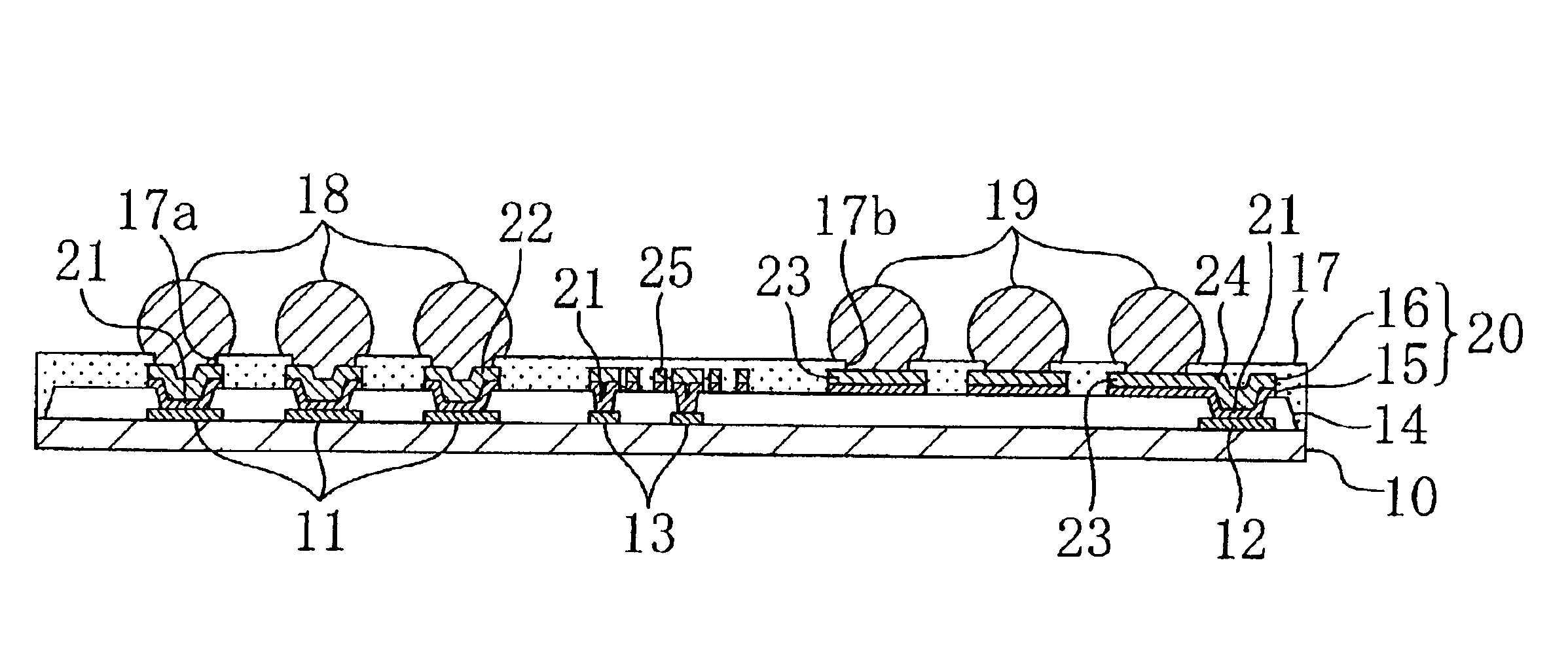
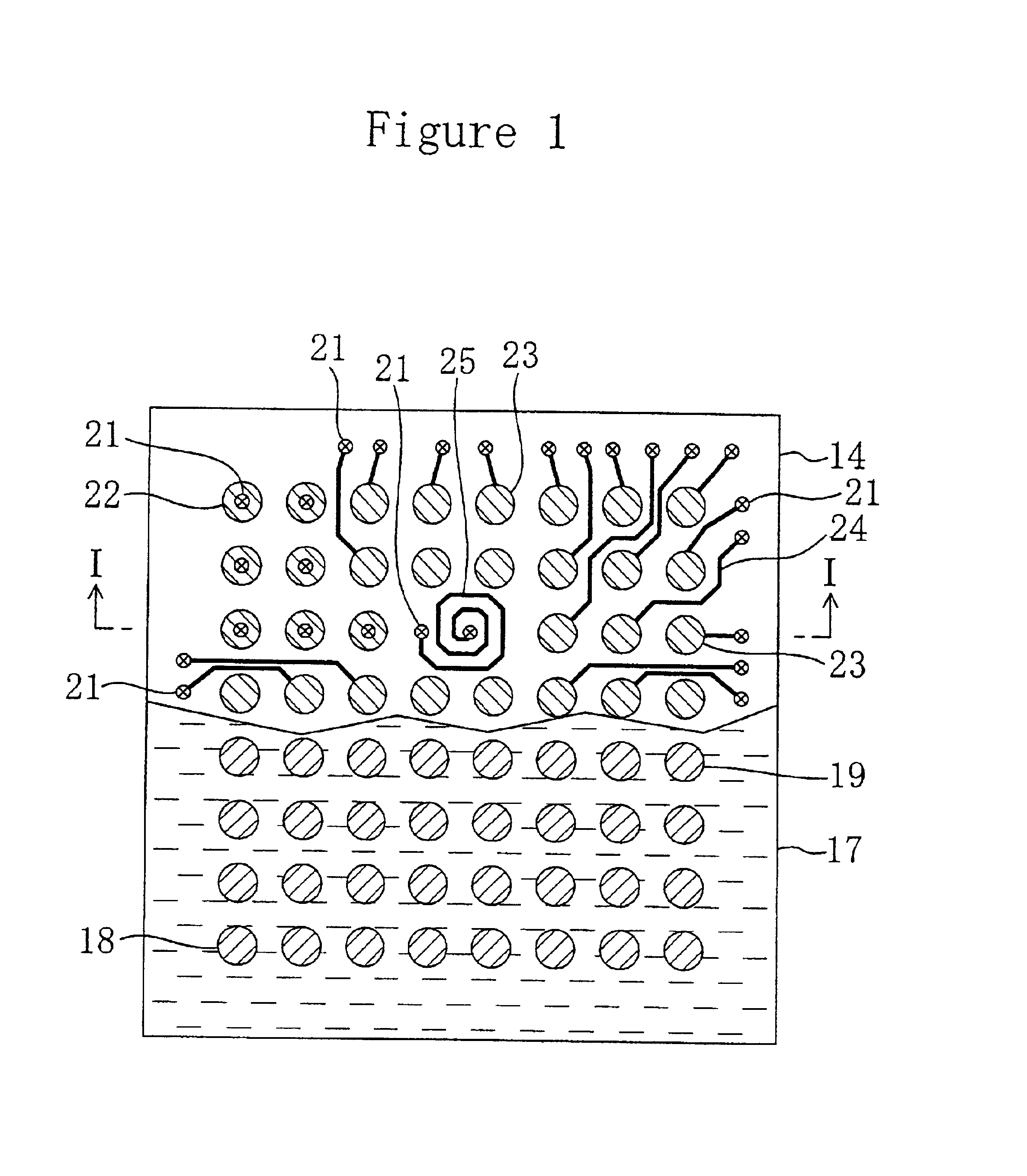
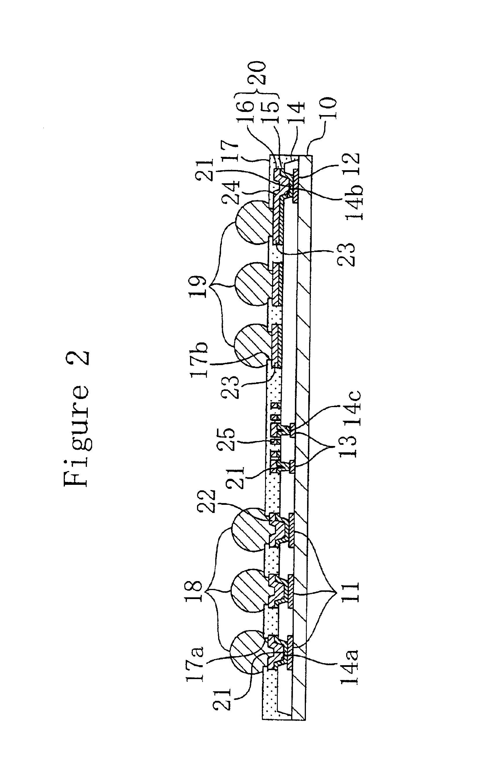
FIG. 1 is a plan view of a semiconductor device according to an embodiment, and FIG. 2 is a cross-sectional view taken along line I—I of FIG. 1. FIG. 1 is a partially cutaway view of the upper side of a semiconductor device according to an embodiment. In FIGS. 1 and 2, although not shown, a semiconductor integrated circuit including at least one semiconductor element such as a transistor is formed on a semiconductor substrate 10. Furthermore, in this embodiment, the semiconductor substrate 10 may be a semiconductor wafer or a chip obtained by dividing a semiconductor wafer.

As shown in FIGS. 1 and 2, a plurality of element electrodes for high-speed signals 11 are provided in the inner portion of a main surface of the semiconductor substrate 10, and a plurality of element elec...


PUM


Abstract

A first element electrode and a second element electrode connected electrically to a semiconductor element on a substrate are formed, and then an insulating film is formed on the substrate including the element electrodes. Thereafter, a first opening for exposing the first element electrode and a second opening for exposing the second element electrode are formed on the insulating film. Then, a first external electrode connected to the first element electrode via the first opening is formed immediately above the first element electrode. Furthermore, a second external electrode and a connecting wire having one end connected to the second element electrode via the second opening and the other end connected to the second external electrode are formed on the insulating film.

Description

BACKGROUND OF THE INVENTIONThe present invention relates to a semiconductor device and a method for producing the same that has a built-in integrated circuit section used for information communication equipment or electronic equipment for offices and allows a high-density packaging provided with wires or electrodes that connect the semiconductor integrated circuit section to the terminals of external equipment.Recently, with compactness, high density and high functionality of electronic equipment, compactness and high density have been required for semiconductor devices. To satisfy this need, a technique to form CSP (chip size package) within semiconductor wafers has come to be used (Japanese Laid-Open Patent Publication No. 8-102466). The CSP formed within a semiconductor wafer is called a wafer level CSP even after a semiconductor wafer is divided into chips.Hereinafter, a conventional semiconductor device and a production method thereof will be described in detail in reference wi...

Claims


Application Information

Patent Timeline
Patent Type & Authority Patents(United States)
IPC IPC(8): H01L23/28H01L23/31H01L23/522H01L23/48H01L23/485H01L23/52H01L21/3205H01L23/12
CPCH01L23/3114H01L23/522H01L24/13H01L23/5227H01L24/10H01L2924/0002H01L2224/0401H01L2924/00014H01L2224/45147H01L2224/45124H01L2224/05572H01L2224/05567H01L2224/05027H01L2924/014H01L2924/01033H01L2924/01024H01L2924/01006H01L2224/13099H01L2924/01004H01L2924/01013H01L2924/01022H01L2924/01029H01L2924/01074H01L2924/01078H01L2924/01079H01L2924/14H01L2924/30107H01L2924/01005H01L2924/00H01L2224/48H01L2224/05552H01L2924/12042H01L2224/13H01L2924/00011H01L2224/05144H01L2224/05155H01L2224/05166H01L2224/05171H01L2224/05184H01L2224/05644H01L2224/05647H01L2224/05655H01L2224/05666H01L2224/05671H01L2224/05684H01L2224/06131H01L24/05H01L2224/023H01L2924/013H01L2924/0001
Inventor SAHARA, RYUICHIWATASE, KAZUMIKUMAKAWA, TAKAHIROKAINOH, KAZUYUKISHIMOISHIZAKA, NOZOMI
Owner TESSERA ADVANCED TECH
Why Eureka
Try Eureka