Stacked semiconductor package

Active Publication Date: 2006-09-21
CANON KK
View PDF2 Cites 49 Cited by
  • Summary
  • Abstract
  • Description
  • Claims
  • Application Information

AI Technical Summary

Benefits of technology

[0016] The present invention has been made in view of the problems described in the above. Therefore, an object of the present inventi

Problems solved by technology

Also, in recent years, as the electronic equipment grows more sophisticated, the electric circuits used therein become increasingly larger in size.
Therefore, fluctuation of its in

Method used


Image

  • Stacked semiconductor package
  • Stacked semiconductor package
  • Stacked semiconductor package

Examples


Example

First Embodiment

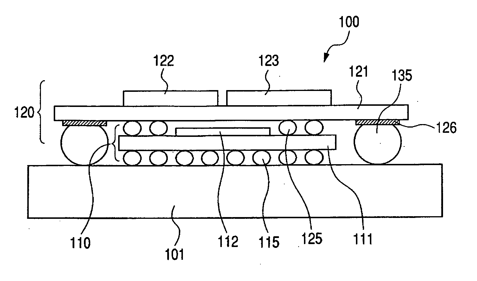
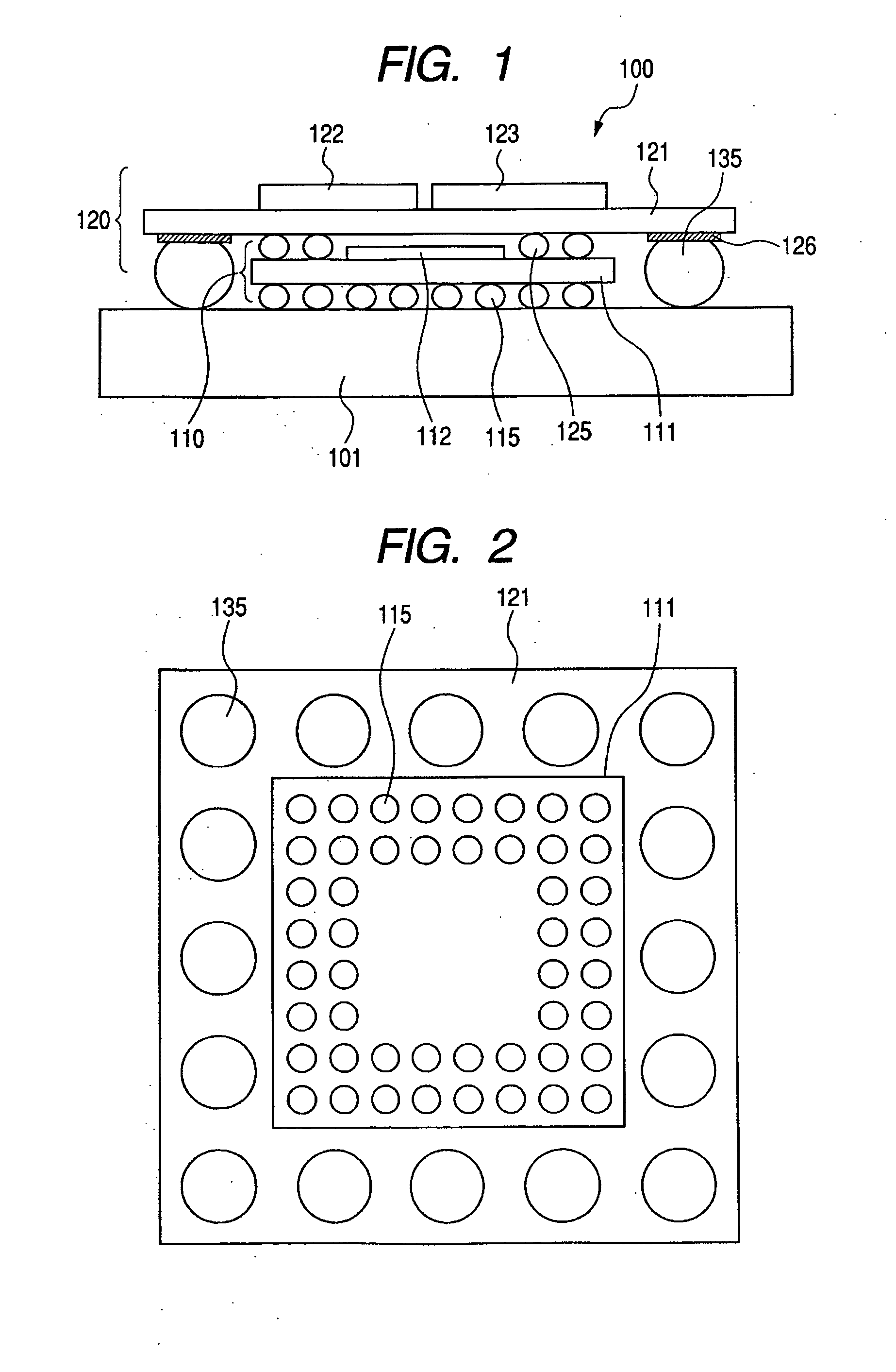
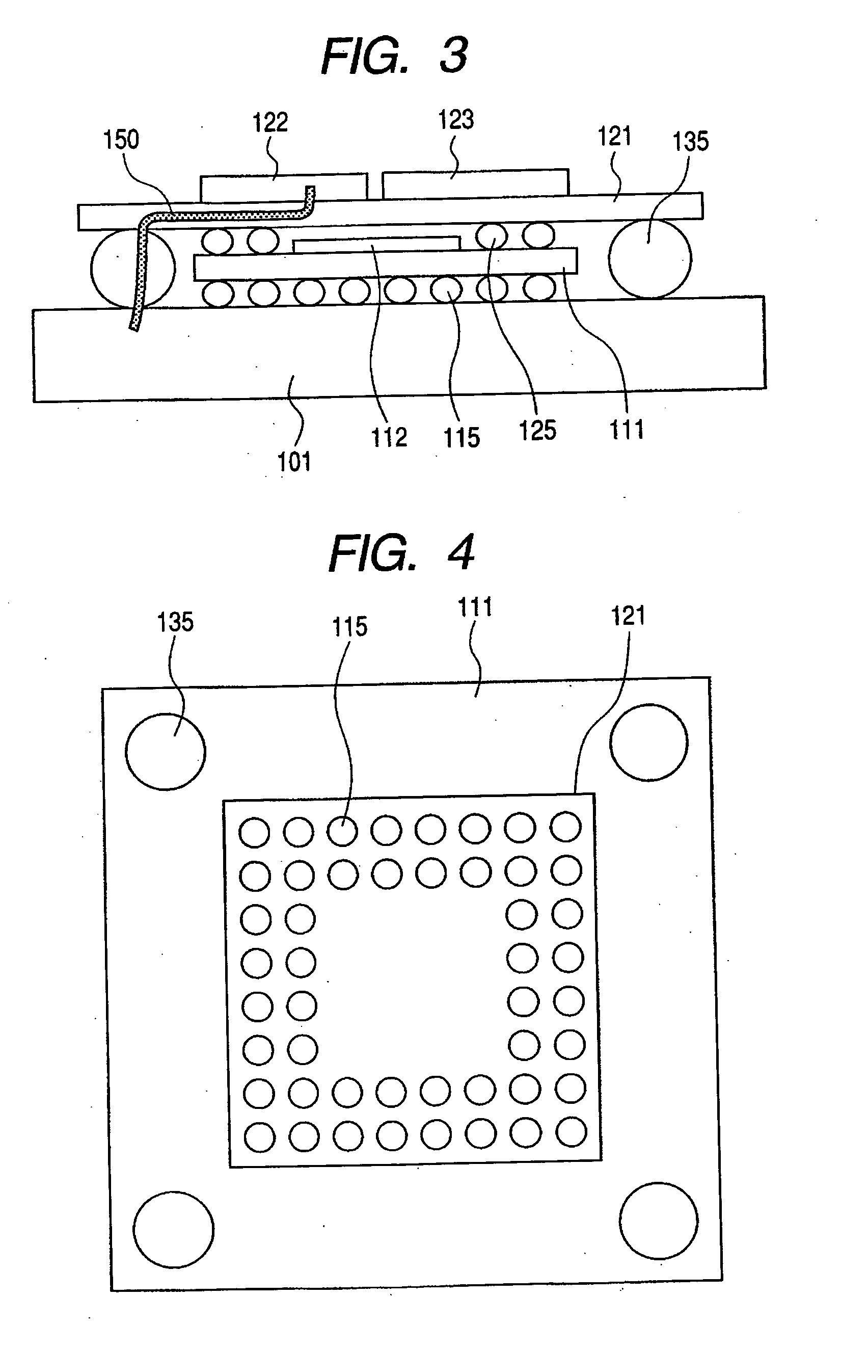
[0080]FIG. 1 is a sectional view of a stacked semiconductor package 100 according to first Embodiment of the present invention. In FIG. 1, the stacked semiconductor package 100 is mounted on a printed wiring board 101. The stacked semiconductor package 100 has a two-layer structure composed of a first semiconductor package 110 and a second semiconductor package 120.

[0081] The first semiconductor package 110 is formed of a square-shaped first package substrate 111, a first LSI 112, and a solder ball group 115. The first LSI 112 is mounted on an upper surface of the first package substrate 111 by a flip chip method. The LSI 112 is a LOGIC circuit which is responsible for the functionality of the product. A solder ball group 115 for electrically connecting the first package substrate 111 and the printed wiring board 101 is provided on a lower surface of the first package substrate 111.

[0082] The second semiconductor package 120 is formed of a square-shaped second pac...

Example

Second Embodiment

[0094]FIG. 8 is a schematic view of a stacked semiconductor package 200 according to second Embodiment of the present invention. FIG. 8A is a sectional view of the stacked semiconductor package 200 and FIG. 8B is a plan view seen from the bottom. The stacked semiconductor package 200 has a two-layer structure composed of a first semiconductor package 210 and a second semiconductor package 220.

[0095] The first semiconductor package 210 is formed of a first package substrate 211, a first LSI 212, and a solder ball group 215. The first LSI 212 is mounted on an upper surface of the first package substrate 211 by a flip chip method. The LSI 212 is an MPU circuit which is responsible for the functionality of a product. A solder ball group 215 for electrically connecting the first package substrate 211 and the printed wiring board (not shown) is provided on a lower surface of the first package substrate 211.

[0096] The second semiconductor package 220 is formed of a seco...

Example

Third Embodiment

[0106]FIGS. 10A and 10B are schematic views of a stacked semiconductor package 300 according to third Embodiment of the present invention. FIG. 10A is a sectional view of the stacked semiconductor package 300 and FIG. 10B is a plan view seen from the bottom. The stacked semiconductor package 301 has a two-layer structure composed of a first semiconductor package 310 and a second semiconductor package 320.

[0107] The first semiconductor package 310 is formed of a first package substrate 311, a first LSI 312. The first LSI 312 is mounted on an upper surface of the first package substrate 311 by a flip chip method. The LSI 312 is an MPU circuit which is responsible for the functionality of the product. A lower surface of the first package substrate 311 is electrically connected to the printed wiring board (not shown) through a solder ball group 315.

[0108] The second semiconductor package 320 is formed of a second package substrate 321, a flash memory 322 as a second L...


PUM


Abstract

In a stacked semiconductor package, since electric power is supplied to a second semiconductor package through a first semiconductor package, a power supply path becomes complicated and fluctuation of its inductance becomes large, whereby power bounce occurs to reduce signal quality and also prevent high speed signal communication. Therefore, according to the present invention, a first solder ball group for joint to a printed wiring board is attached to a second layer of the first semiconductor package, and a second solder ball group for joint to the first semiconductor package and a solder group for power supply for direct joint to the printed wiring board are provided on the second layer of the second semiconductor package, whereby electric power can be directly supplied from the printed wiring board.

Description

BACKGROUND OF THE INVENTION [0001] 1. Field of the Invention [0002] The present invention relates to a stacked semiconductor package obtained by three-dimensionally stacking a plurality of semiconductor packages each having at least one semiconductor chip mounted thereon. [0003] 2. Related Background Art [0004] Up to now, a semiconductor package to be used in an electronic equipment adopts a ball grid array (BGA) in which lands are formed in a grid pattern or a chip scale package (CSP) to thereby attain electronic equipments with a smaller size and a higher performance. Also, in recent years, as the electronic equipment grows more sophisticated, the electric circuits used therein become increasingly larger in size. Accordingly, in order to materialize an electric circuit with high density, a stacked semiconductor package in which semiconductor packages are three-dimensionally stacked is gradually used. [0005] A system in package (SIP) structure and a package on package (POP) structu...

Claims


Application Information

Patent Timeline
IPC IPC(8): H01L23/02
CPCH05K2201/10734H01L2224/97H01L2924/15311H01L24/97H01L25/0657H01L25/105H01L2224/32145H01L2224/48225H01L2225/06568H01L2924/01027H01L2924/01029H01L2924/01047H01L2924/01082H01L2924/15331H01L2924/19041H01L2924/19043H01L2924/19105H01L2924/30107H05K1/0263H05K1/141H05K1/145H05K3/3436H05K2201/10515H01L2924/01005H01L2924/01006H01L2924/01019H01L2924/01033H01L2225/1023H01L2225/1058H01L2224/16225H01L2224/48227H01L2924/00011H01L2924/00014H01L2924/181H01L2924/00H01L2224/0401
Inventor OHSAKA, TOHRUKONDO, HIROSHI
Owner CANON KK
Why Eureka
Try Eureka