Optical device, optical device manufacturing method, and optical integrated device

a technology of optical transmission line and optical integrated device, which is applied in the direction of optical waveguide light guide, instruments, optics, etc., can solve the problems of large loss of coupling to the optical transmission line provided on the exit side, inability to perform transmission at a high speed exceeding 10 gbps, and limited transmission speed, etc., to achieve excellent demultiplexing performance, easy coupling and small loss

Active Publication Date: 2005-11-24
PANASONIC CORP
View PDF9 Cites 46 Cited by
  • Summary
  • Abstract
  • Description
  • Claims
  • Application Information

AI Technical Summary

Benefits of technology

[0036] Moreover, in the optical waveguides described in Documents (4) to (8) and (11), when a signal beam that is single-mode in the direction of the thickness is made incident, the coupling loss is small and the signal beam can be transmitted at high speed. However, even in the case of a single mode, when an incident beam largely diffused and having a large spread angle or an incident beam with a large beam diameter such as an exiting beam from a multi-mode waveguide is used as the signal beam, since the coupling to the optical waveguide is difficult, the loss of the signal beam when the signal beam is incident and exits is large. Moreover, in the optical waveguide described in Documents (4) to (8) and (11), since loss is large with respect to the incident beam that is incident with its axis being shifted from the center of the optical waveguide, it is necessary to couple the incident and exiting beams to the incident and exit sides with high accuracy.
[0350] According to this structure, the signal beam incident on the optical transmission line from a direction not parallel to the second direction can be easily made incident on the optical transmission line. Moreover, the signal beam exiting from the optical transmission line in a direction not parallel to the second direction can be easily made to exit from the optical transmission line.

Problems solved by technology

Therefore, in the multi-mode optical transmission lines described in Documents (2) and (3), the transmission speed is limited by the typical incident beam dispersion, so that transmission at a high speed exceeding 10 Gbps cannot be performed.
However, since the refractive index is uniform in the direction of the width, the mode dispersion in the direction of the width occurs, so that the transmission speed is limited as well.
Moreover, in all of the technologies described in Documents (1) to (3), since the incident beam exits from the entire area of the exit side end surface as the exiting beam, the loss of coupling to the optical transmission line provided on the exit side is large.
However, even in the case of a single mode, when an incident beam largely diffused and having a large spread angle or an incident beam with a large beam diameter such as an exiting beam from a multi-mode waveguide is used as the signal beam, since the coupling to the optical waveguide is difficult, the loss of the signal beam when the signal beam is incident and exits is large.
Moreover, when the optical waveguides described in Documents (4) to (8) and (11) are used with a signal beam that is multi-mode in the direction of the thickness being made incident, the problem is improved that it is difficult to couple the incident and exiting beams with respect to the incident beam largely diffused and having a large spread angle and the incident beam with a large beam diameter.
However, when the optical waveguides described in Documents (4) to (8) and (11) are used with a signal beam that is multi-mode in the direction of the thickness being made incident, the mode dispersion occurs in the direction of the thickness, so that the signal beam cannot be transmitted at high speed.

Method used


Image

  • Optical device, optical device manufacturing method, and optical integrated device
  • Optical device, optical device manufacturing method, and optical integrated device
  • Optical device, optical device manufacturing method, and optical integrated device

Examples


fifth embodiment

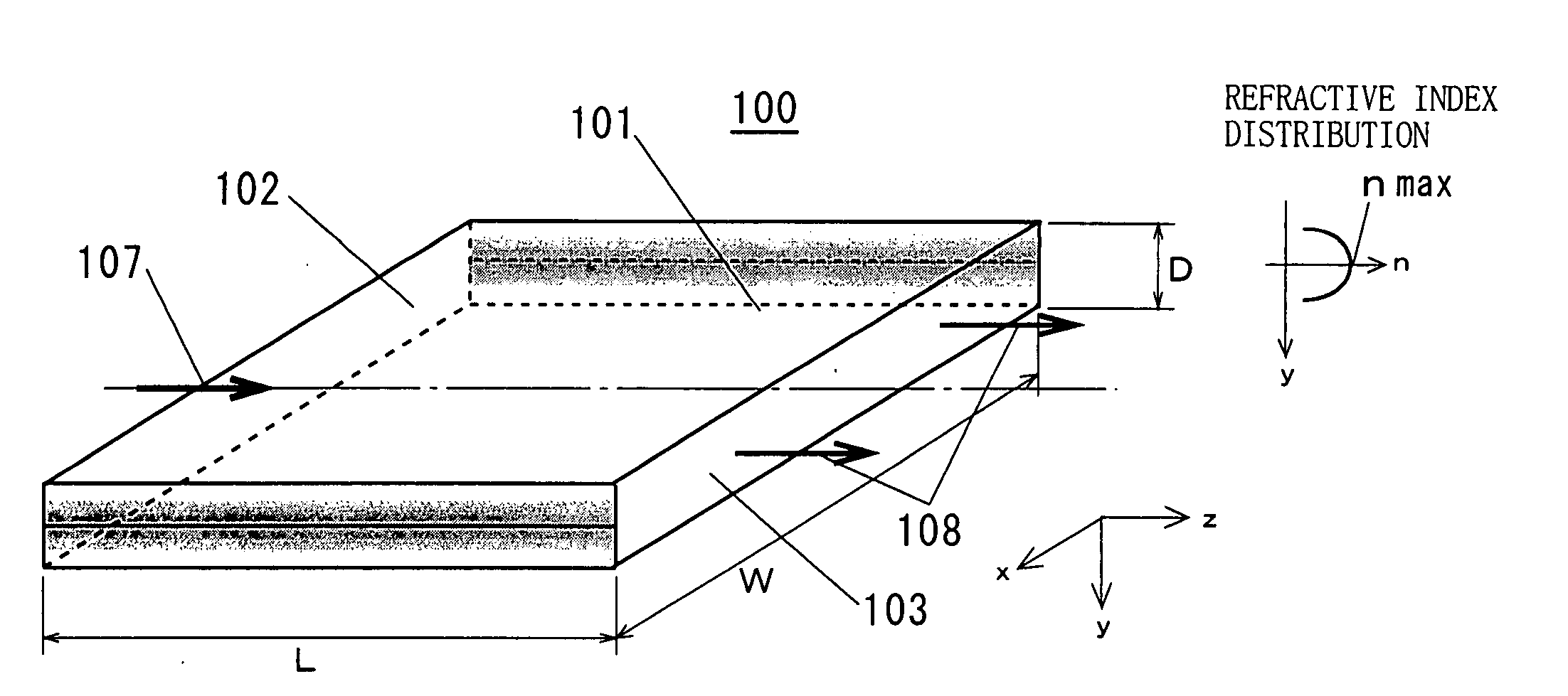
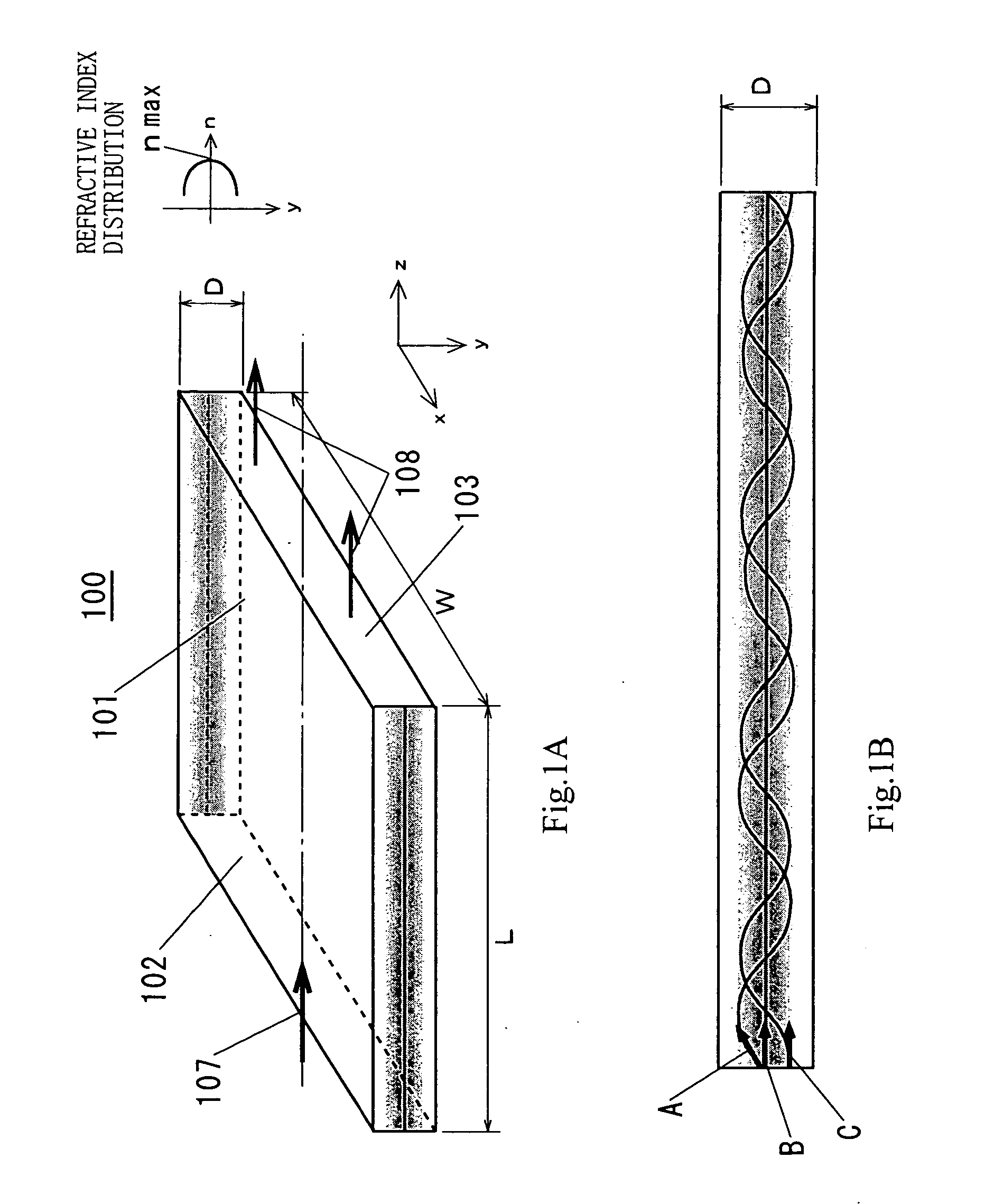
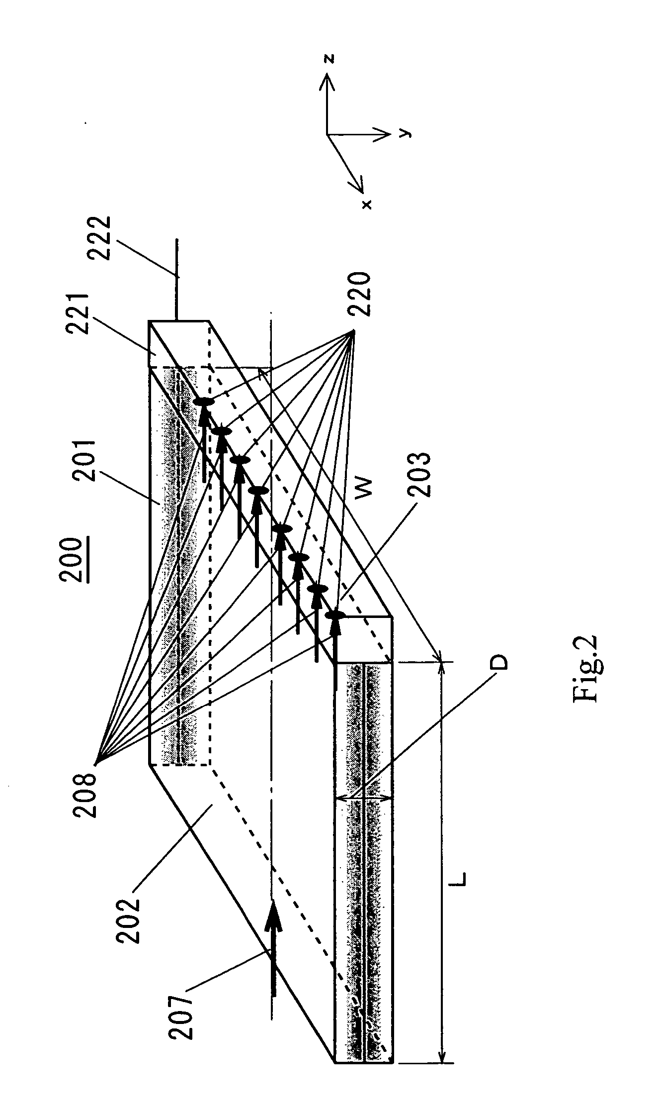
[0471]FIG. 7 is a perspective view showing the general outline of a two-signal star coupler which is an optical device according to a fifth embodiment of the present invention. The optical device according to the fifth embodiment comprises as a main element a graded index slab waveguide 701 that transmits beams. The graded index slab waveguide 701 is, as shown in FIG. 7, a sheet-form multi-mode optical transmission line that extends parallel to the x-z plane. The graded index slab waveguide 701 has a distribution such that the highest refractive index nmax is provided at the center in the direction of the thickness and the refractive index does not increase with distance from the center. The graded index slab waveguide 701 has a uniform refractive index in the direction of the width and has no refractive index distribution. The optical device according to the fifth embodiment is provided with an array E / O converter 732, an input electric line (bus) 333, an array O / E converter 736 an...

sixth embodiment

[0481]FIG. 8A is a perspective view showing the general outline of a one side control type optical switch which is an optical device according to a sixth embodiment of the present invention. The optical device according to the sixth embodiment comprises as main elements a first graded index slab partial waveguide 801a and a second graded index slab partial waveguide 801b that transmit beams. The first graded index slab partial waveguide 801a and the second graded index slab partial waveguide 801b are both sheet-form multi-mode optical transmission lines that extend parallel to the x-z plane as shown in FIG. 8A. The first graded index slab partial waveguide 801a and the second graded index slab partial waveguide 801b have the same size in the direction of the width. The first graded index slab partial waveguide 801a and the second graded index slab partial waveguide 801b are disposed so as to be connected continuously in the direction of the width. Moreover, the first graded index sl...

seventh embodiment

[0496]FIG. 9 is a perspective view showing the general outline of an optical switch array which is an optical integrated device according to a seventh embodiment of the present invention. The optical switch array of the seventh embodiment is provided with a laminated optical switch group 901 in which eight optical switches that are described in the first modification of the sixth embodiment (FIG. 8B) are laminated in the direction of the thickness of the graded index slab waveguide 801. In each of the optical switches included in the laminated optical switch group 901, the part corresponding to the first graded index slab partial waveguide 801a described in the sixth embodiment is disposed on the lower side in the figure. The optical integrated device according to the seventh embodiment includes a first array O / E converter 905, a second array O / E converter 906, a first output electric line (bus) 907 and a second output electric line (bus) 908.

[0497] The first array O / E converter 90...


PUM

PropertyMeasurementUnit
thicknessaaaaaaaaaa
lengthaaaaaaaaaa
refractive indexaaaaaaaaaa

Abstract

In a multi-mode interference waveguide (MMI) of a sheet shape spreading in the length direction and the width direction, the length of the multi-mode interference waveguide is set to such a length that the unique mode interferes in the length direction, thereby reducing the coupling loss when inputting / outputting the signal light. The multi-mode interference waveguide has a maximum refraction factor portion in the thickness direction and has such a refraction factor distribution that the refraction factor is reduced as departing from the maximum refraction factor portion. Thus, it is possible to suppress mode dispersion in the thickness direction of the multi-mode interference waveguide and obtain a high transmission rate in the order of 10 Gb / s.

Description

TECHNICAL FIELD [0001] The present invention relates to an optical device having a sheet-form transmission line used for high-speed multi-mode optical transmission and a method of manufacturing the optical device, and more specifically, to an optical device using a self-imaging principle of a multi-mode interference suitable for an optical splitter, an optical combiner, an optical demultiplexer, an optical multiplexer, an optical straight sheet bus, an optical cross sheet bus, a star coupler, an optical switch and the like, and a method of manufacturing the optical device. Moreover, the present invention relates to an optical integrated device having the above-described optical device in a plurality of numbers. BACKGROUND ART [0002] Research has been performed on an optical device using an optical transmission line which optical device is suitable for optical communication systems and the like. It is expected that such an optical device will be applied to an optical data bus sheet f...

Claims


Application Information

Patent Timeline
Patent Type & Authority Applications(United States)
IPC IPC(8): G02B6/12G02B6/138G02B6/28G02B6/30G02B6/42G02F1/313
CPCG02B6/138G02B6/2813G02B6/30G02F2001/217G02B2006/12095G02F1/3136G02F1/3137G02B6/4214G02F1/217G02B6/24G02B6/28
Inventor HAMADA, HIDENOBU
Owner PANASONIC CORP
Why Eureka
Try Eureka