Optical device

a technology of optical devices and optical light guides, applied in the field of optical devices, can solve the problems of affecting the refractive index profile, and incurred coupling loss of approximately 2 db in total at the input and output parts,

Inactive Publication Date: 2007-11-29
FUJITSU LTD
View PDF5 Cites 5 Cited by
  • Summary
  • Abstract
  • Description
  • Claims
  • Application Information

AI Technical Summary

Benefits of technology

[0023]Another and more specific object of the present invention may be to provide an optical device having a structure where the light intensity distribution of an optical waveguide is substantially consistent with the light intensity distribution of an optical fiber for at least one of optical input and output parts (parts connecting the optical device and the optical fiber) and therefore there is little coupling loss.
[0030]According to an embodiment of the present invention, it is possible to provide the optical device having the structure where the light intensity distribution of the optical waveguide is substantially consistent with the light intensity distribution of the optical fiber for at least one of the optical input and output parts (the parts connecting the optical device and the optical fibers) and therefore there is little coupling loss.

Problems solved by technology

However, in order to use the optical device using such a diffusion waveguide (optical waveguide) in an optical fiber transmission system, it is necessary to consider the coupling loss with the optical fiber.
Because of this, when the diffusion waveguide is inserted between the optical fibers, coupling loss of approximately 2 dB in total at the input and output parts may be incurred.
Therefore, it is difficult to achieve a desirable refractive index profile.

Method used


Image

  • Optical device
  • Optical device
  • Optical device

Examples


first embodiment

1. First Embodiment of the Present Invention

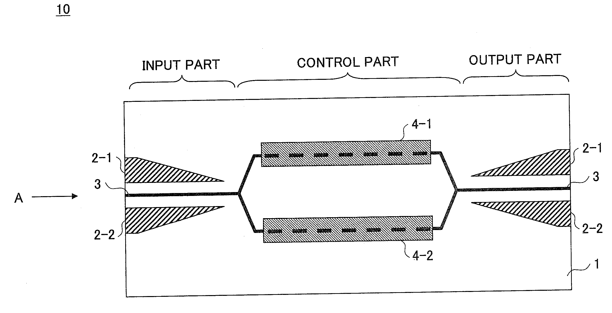
[0046]FIG. 3 is a plan view showing a schematic structure of an optical device of a first embodiment of the present invention. FIG. 4 is a schematic view seen in a direction shown by an arrow A of the optical device shown in FIG. 3.

[0047]In FIG. 3 and FIG. 4, an example where the present invention is applied to a Mach-Zehnder type optical modulator is shown as an optical device 10.

[0048]Referring to FIG. 3, the Mach-Zehnder type optical modulator is formed as the optical device 10. The optical device 10 has a structure where a waveguide (optical waveguide) 3 is formed on a dielectric substrate 1 having a photoelastic effect such as lithium niobate (LiNbO3). The waveguide (optical waveguide) 3 is made by diffusing metal atoms such as titanium (Ti).

[0049]The dielectric substrate 1 made of lithium niobate (LiNbO3), as well as a substrate made of lithium tantalate (LiTaO2) discussed below, have large electrooptic coefficients. Hence, it is pos...

second embodiment

2. Second Embodiment of the Present Invention

[0072]FIG. 6 is a plan view showing a schematic structure of an optical device of a second embodiment of the present invention. FIG. 7 is a schematic view seen in a direction shown by an arrow A of the optical device shown in FIG. 6. In FIG. 6 and FIG. 7, parts that are the same as the parts shown in the first embodiment of the present invention are given the same reference numerals, and explanation thereof is omitted.

[0073]In the above-discussed first embodiment of the present invention, as shown in FIG. 4, the stress layers 2-1 and 2-2 are patterned and provided at the input and output parts so that the diffusion waveguide 3 is put between the stress layers 2-1 and 2-2. On the other hand, in the second embodiment of the present invention, as shown in FIG. 6 and FIG. 7, patterning reverse of the patterning in the first embodiment of the present invention is made. A stress layer 22 is provided on the diffusion waveguide 3 and makes the di...

third embodiment

3. Third Embodiment of the Present Invention

[0104]In the above-discussed embodiments of the present invention, the present invention is applied to the waveguide (mainly, diffusion waveguide) wherein the distribution of the light intensity is leaned toward the surface of the substrate.

[0105]However, the present invention is not limited to these examples. The present invention may be applied to other asymmetric optical waveguides. For example, a three dimensional optical waveguide can be formed at an optical depth of the substrate by making convergent radiotherapy of a high intensity laser such as Femto second laser to the dielectric substrate. In this case, generally, the formed optical waveguide has an elliptic-shaped configuration.

[0106]An example of a case where the present invention is applied to an elliptic waveguide having optional depth is shown in FIG. 12. Here, FIG. 12 is a cross-sectional view of input and output parts of an optical device of a third embodiment of the prese...


PUM


Abstract

An optical device wherein an optical waveguide is formed on a dielectric substrate, the optical device includes an input part and an output part where the optical waveguide and corresponding optical fibers are connected. A stress layer is provided for at least one of the input part and the output part. The stress layer applies a stress to the optical waveguide so that an index of refraction of the optical waveguide is reduced.

Description

BACKGROUND OF THE INVENTION[0001]1. Field of the Invention[0002]The present invention generally relates to optical devices, and more specifically, to an optical device used in technical fields such as optical communication or optical signal processing.[0003]2. Description of the Related Art[0004]As for recent and continuing development of optical communication systems, a system having a large capacity and high functions has been requested. Hence, it is required to develop an optical device such as an optical switch or modulator for high speed optical wave. In such an optical device, not only high speed but also low loss or low voltage is required.[0005]As the high speed optical device, for example, an optical switch, an optical modulator, and an optical control element are reported wherein a waveguide is formed in a substrate made of a crystal of lithium niobate (LiNbO3) having a large electrooptic coefficient and the change of the index of refraction of the waveguide is controlled ...

Claims


Application Information

Patent Timeline
Patent Type & Authority Applications(United States)
IPC IPC(8): G02B6/26
CPCG02F1/225G02B6/305
Inventor SHIRAISHI, TAKASHI
Owner FUJITSU LTD
Why Eureka
Try Eureka