Semiconductor device and manufacturing method therefor, circuit board, and electronic equipment

a semiconductor and manufacturing method technology, applied in the direction of semiconductor devices, semiconductor/solid-state device details, electrical apparatus, etc., can solve the problems of difficult to guarantee reliable electrical connection, limit of miniaturization of wires and similar components, etc., to suppress any drop in the strength of the semiconductor element, the effect of stress

Inactive Publication Date: 2005-02-08
ADVANCED INTERCONNECT SYST LTD
View PDF19 Cites 81 Cited by
  • Summary
  • Abstract
  • Description
  • Claims
  • Application Information

AI Technical Summary

Benefits of technology

Since this ensures that the width of the intermediate portion is substantially uniform over all portions thereof, stresses are made uniform and it is possible to suppress any drop in the strength of the semiconductor element due to the formation of the through-hole.

Problems solved by technology

In many cases, electrical connections are intended to be done by bonding wires or leads to electrodes of the semiconductor chips, but the limit of miniaturization has been reached for the provision of wires and similar components.
However, voids occur when solder is poured into tiny through-holes, making it difficult to guarantee reliable electrical connections

Method used


Image

  • Semiconductor device and manufacturing method therefor, circuit board, and electronic equipment
  • Semiconductor device and manufacturing method therefor, circuit board, and electronic equipment
  • Semiconductor device and manufacturing method therefor, circuit board, and electronic equipment

Examples


Embodiment Construction

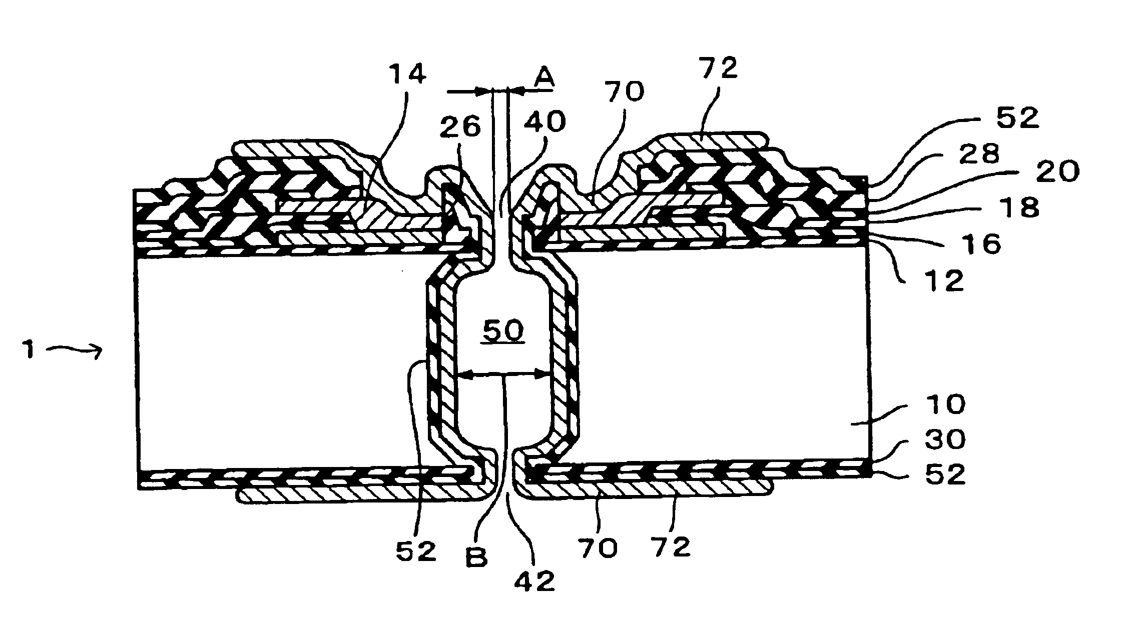
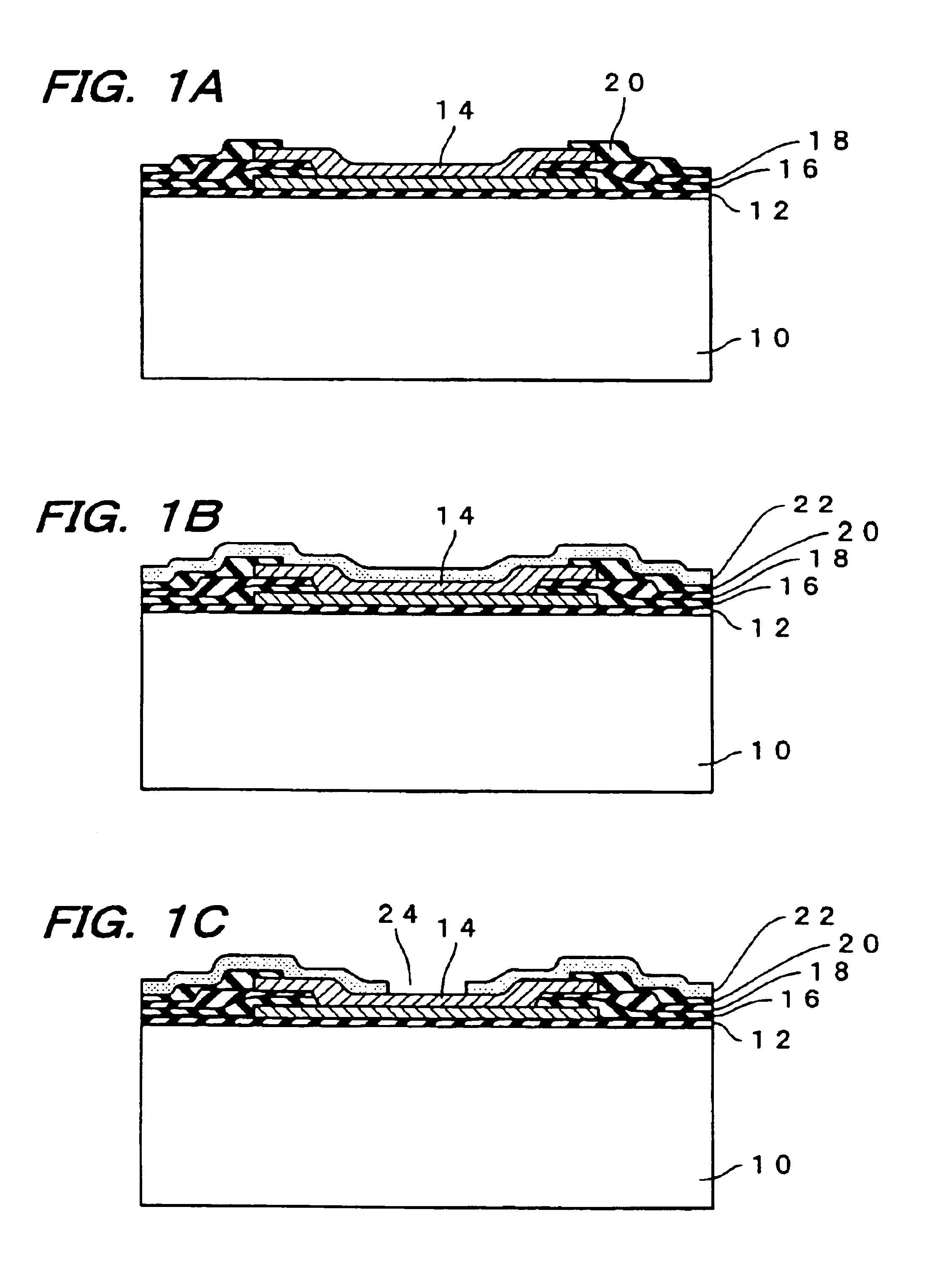
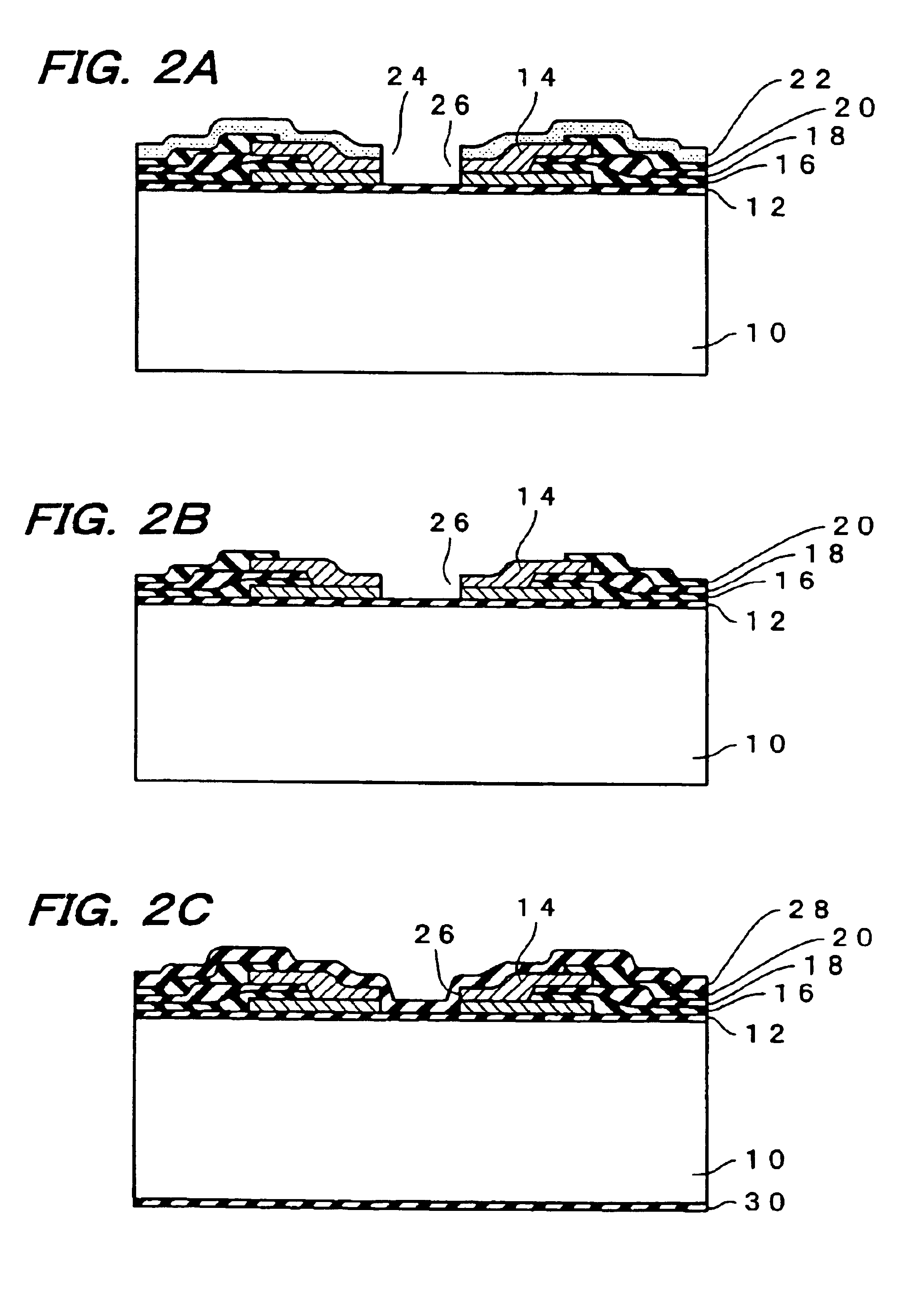
Preferred embodiments of the present invention are described below with reference to the accompanying figures. FIGS. 1A to 9 show sectional views of a semiconductor chip of which the direction of sight crosses the thickness direction of the semiconductor chip. Part of a semiconductor chip 10 used by this embodiment is shown in FIG. 1A. The semiconductor chip 10 is generally of a rectangular parallelepiped shape (including a cube), but the shape is not limited thereto and it could also be a sphere.

The semiconductor chip 10 has an insulation film (inter-layer film) 12 on a surface on which an integrated circuit formed of transistors and memory elements (not shown in the figure) are formed. This insulation film 12 is often an oxidized film of the silicon that is the basic material of the semiconductor chip 10. Electrodes (pads) 14 are formed on the insulation film 12 and these electrodes 14 are connected electrically to an integrated circuit by portions that are not shown in the figure...


PUM


Abstract

A method of manufacturing a semiconductor device comprises a step of forming a through-hole in a semiconductor chip having an electrode and forming a conductive layer on a region comprising an inner side of the through-hole. An intermediate portion of the through-hole is formed to be larger than an edge portion thereof, and the conductive layer is formed by electroless plating.

Description

BACKGROUND OF THE INVENTION1. Field of the InventionThe present invention relates to a semiconductor device and manufacturing method therefor, a circuit board, and electronic equipment.2. Description of the Related ArtSemiconductor devices have recently been developed in which a plurality of semiconductor chips are formed into a stack. In many cases, electrical connections are intended to be done by bonding wires or leads to electrodes of the semiconductor chips, but the limit of miniaturization has been reached for the provision of wires and similar components. Electrical connections have also been developed such that a through-hole is formed in a semiconductor chip, then solder is poured into the through-hole. However, voids occur when solder is poured into tiny through-holes, making it difficult to guarantee reliable electrical connectionsSUMMARY OF THE INVENTIONThe present invention was devised to solve the above problem and has as an objective thereof the provision of a semicon...

Claims


Application Information

Patent Timeline
Patent Type & Authority Patents(United States)
IPC IPC(8): H01L21/02H01L21/288H01L25/065H01L23/48H01L21/70H01L21/768H01L25/18H01L25/07
CPCH01L21/288H01L21/76898H01L23/481H01L25/0657H01L25/50H01L2924/07811H01L2224/16145H01L2225/06513H01L2225/06541H01L2225/06586H01L2924/01046H01L2924/01078H01L2924/01079H01L2924/3025H01L2924/01019H01L2924/00H01L24/03H01L24/05H01L2224/02381H01L2224/05001H01L2224/05011H01L2224/05022H01L2224/05027H01L2224/05556H01L2224/05567H01L2224/05572H01L2224/13025H01L21/768
Inventor HANAOKA, TERUNAOWADA, KENJIHASHIMOTO, NOBUAKIITO, HARUKIUMETSU, KAZUSHIGEMATSUSHIMA, FUMIAKI
Owner ADVANCED INTERCONNECT SYST LTD
Why Eureka
Try Eureka