

Integrated circuit leadframes patterned for measuring the accurate amplitude of changing currents
- Summary
- Abstract
- Description
- Claims
- Application Information
AI Technical Summary
Benefits of technology
Problems solved by technology
Method used
Image

Examples
first embodiment
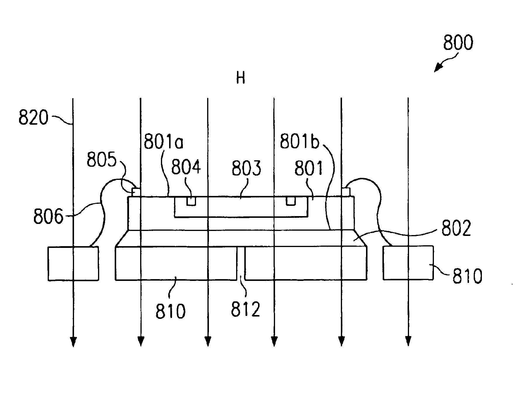
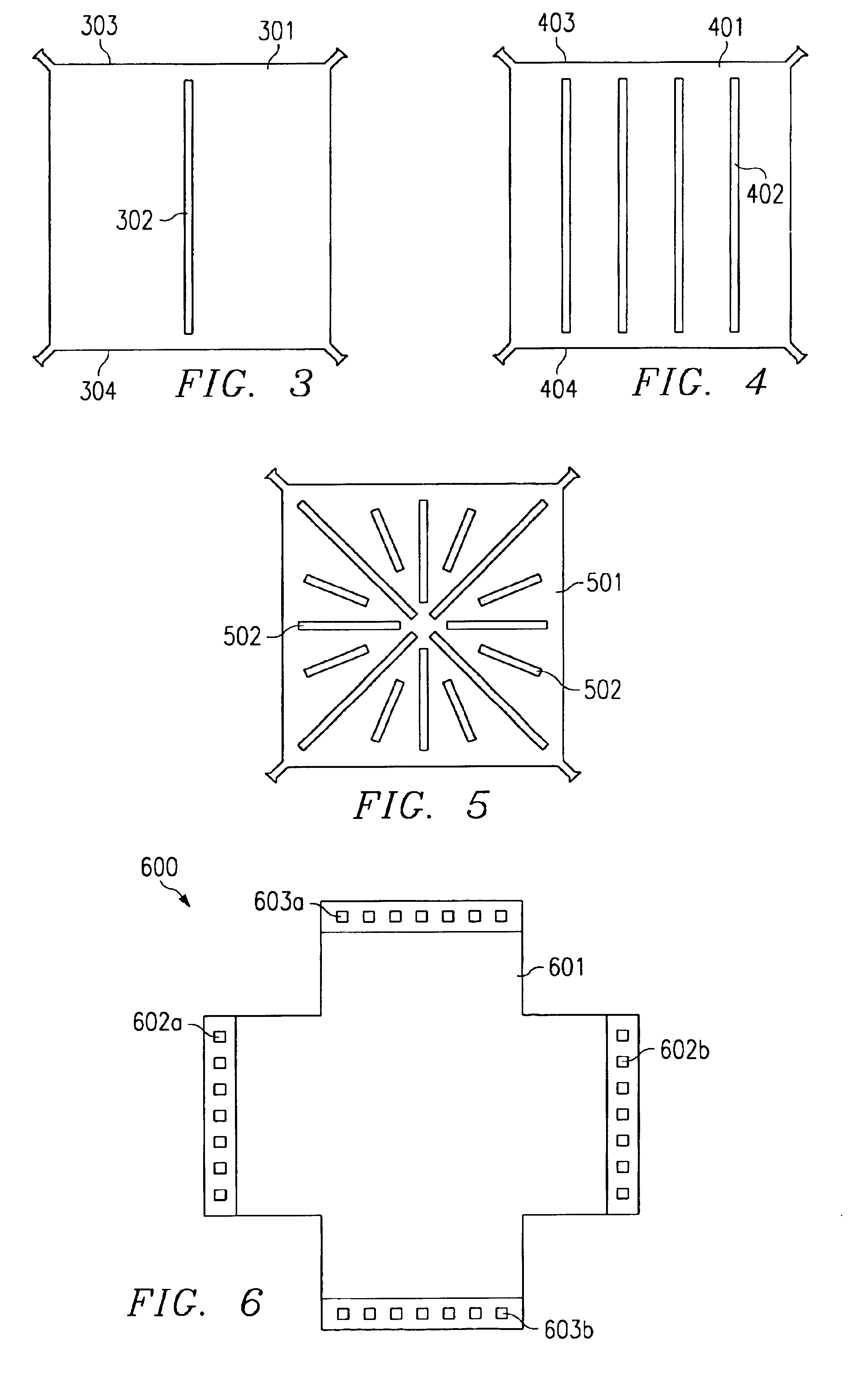
Other variations of slit configurations are shown in FIGS. 3 to 5. FIG. 3 illustrates the top view of an example of the invention. A leadframe chip mount pad 301, which is intended to be operated in a changing magnetic field, has one slit 302 penetrating the whole thickness of the pad metal and substantially traversing the area of the pad from one edge 303 to the opposite edge 304. The width of the slit is in the range from about 0.01 to 0.5 mm, significantly reducing any eddy current induced by the changing magnetic field and flowing in the plane of the pad 301. On the other hand, slit 302 is narrow enough to not interfere with the heat-dissipating capability and thermal conduction in a direction normal to the plane of the pad.
second embodiment
FIG. 4 illustrates the top view of an example of the invention. A leadframe chip mount pad 401, which is intended to be operated in a changing magnetic field, has a plurality of slits 402 arranged in about parallel pattern and penetrating the whole thickness of the pad metal and substantially traversing the area of the pad from one edge 403 to the opposite edge 404. While the widths of the slits 402 do not have to be uniform, they are prefereably on the range from about 0.01 to 0.5 mm. Any eddy current induced by the changing magnetic field and flowing in the plane of pad 401 is strongly suppressed while the narrow widths of the slits do not significantly reduce thermal conduction in a direction normal to the plane of pad 401.
FIG. 5 shows another example of the second embodiment of the invention, a plurality of slits 502 in a leadframe pad 501, arranged in an approximately star-burst-like pattern. As in the previous FIGS. 3 and 4, the slits are about 0.01 to 0.5 mm wide and penetrat...
PUM
 Abstract
Description
Claims
Application Information