Display device

a display device and display screen technology, applied in the field of display devices, can solve the problems of considerable drawback, considerable electric power consumption, and short time a user can use the telephone under one battery charge, and achieve the effects of reducing the size of the pixel element, reducing the size of the signal line, and reducing the spa

Inactive Publication Date: 2005-02-08
SANYO ELECTRIC CO LTD
View PDF17 Cites 146 Cited by
  • Summary
  • Abstract
  • Description
  • Claims
  • Application Information

AI Technical Summary

Benefits of technology

According to the second configuration of this invention, there is provided a display device having a plurality of gate signal lines disposed in a predetermined direction on a substrate, a plurality of drain signal lines disposed in a direction perpendicular to the predetermined direction, a plurality of pixel elements which are disposed as a matrix, activated by the scanning signal fed through the gate signal line and provided with the image signal fed through the drain signal line, a first display circuit which has a storage capacitor element for holding an analog image fed through the drain signal line in response to a signal fed through the gate signal line and supplies the signal held by the storage capacitor element to a pixel electrode, a second display circuit which is disposed near the first display circuit, includes a retaining circuit holding a digital image signal fed through the drain signal line in response to the signal fed through the gate signal line and a signal selection circu

Problems solved by technology

Accordingly, it is necessary to operate a driver circuit which generates a drive signal for the scanning signals and the image signals, and an external LSI which generates various signals for controlling the timing of the drive circuit, resulting in a consumption of a significant amount of electric power.
This is a considerable drawback when such a configuration is used in a cellular phone device, which has

Method used


Image

  • Display device
  • Display device
  • Display device

Examples


first embodiment

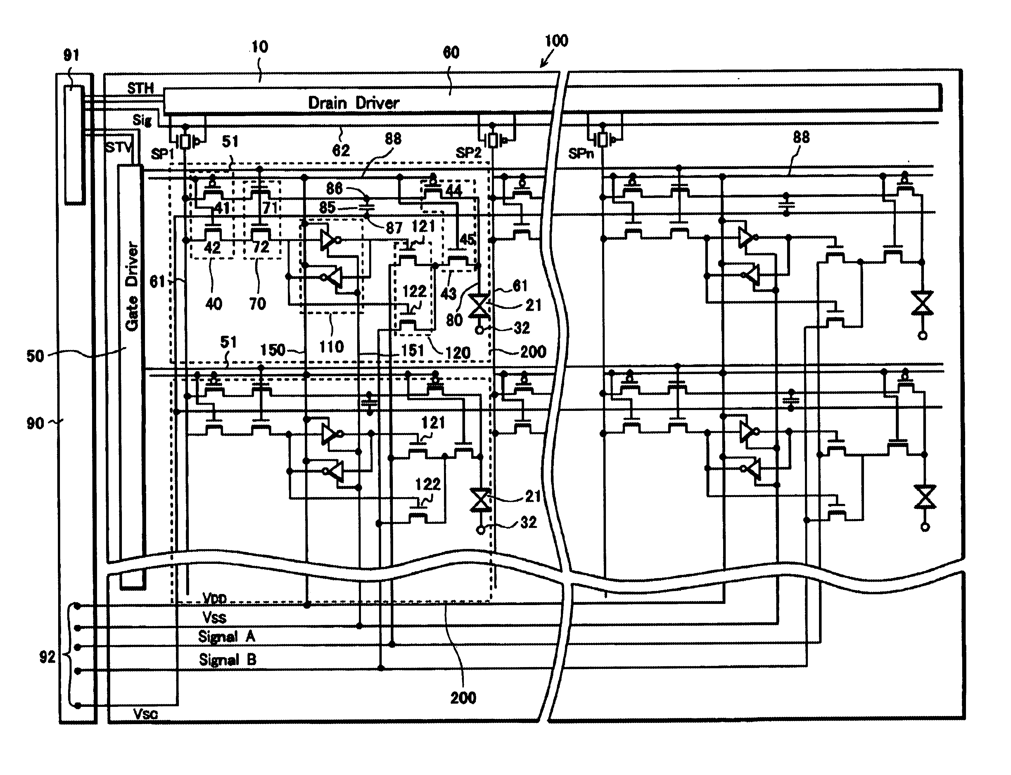
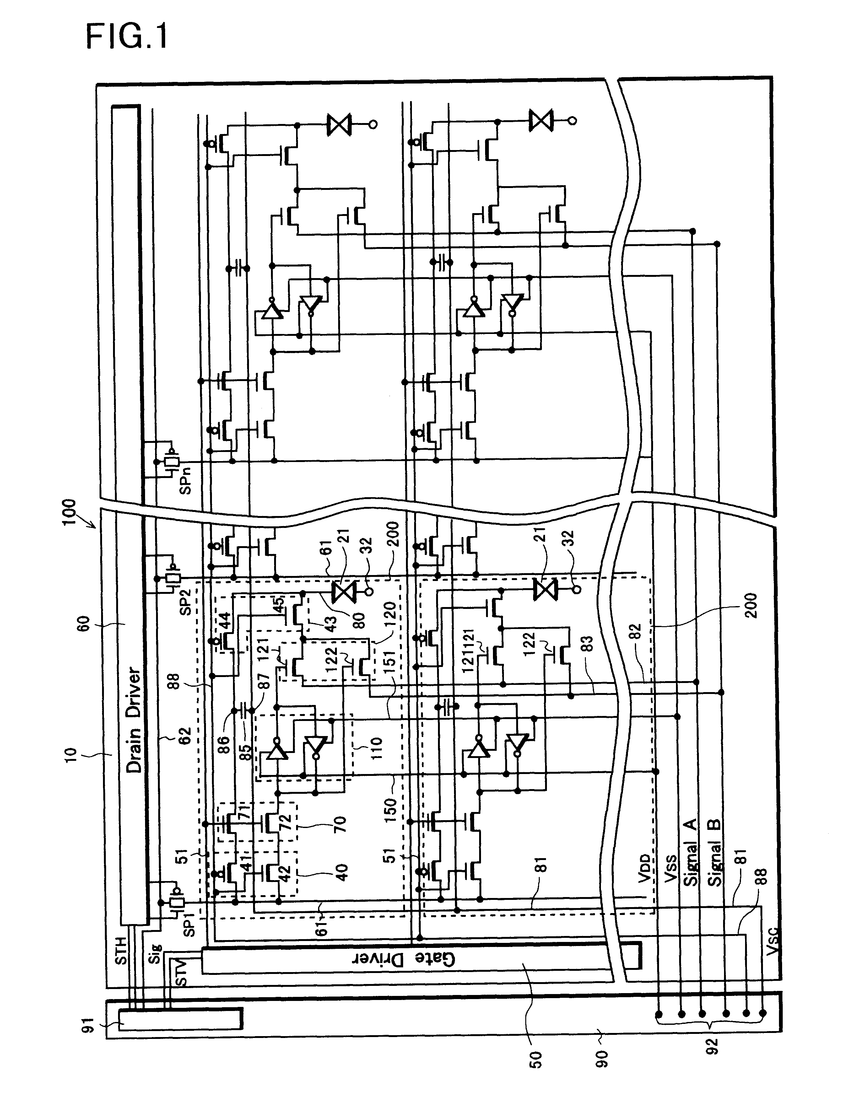
FIG. 3 is a circuit diagram of a liquid crystal display device of this invention. The liquid crystal display device shown in FIG. 1 has an independent wiring for each of the high voltage power line 150 which supplies high voltage Vdd, the low voltage power line 151 which supplies low voltage Vss to the retaining circuit, and the circuit selection signal line 88 provided for the circuit selection circuits 40, 43. Thus, in the area occupied by these lines, the integration of the pixel element 200 is limited to a certain degree.

Thus, as shown in FIG. 3, the circuit selection signal line 88 is cut off from the source of the signal and connected to the high voltage power line 150 of the retaining circuit 110. That is, the high voltage power line 150 of the retaining circuit 110 is extended toward and connected to the circuit selection signal line 88. The part of the circuit selection signal line 88 adjacent to the gate driver 50 is eliminated. And the circuit selection signal line 88 bet...

second embodiment

FIG. 6 is a circuit diagram of a liquid crystal display device of this invention. In the display device shown in FIG. 1, the signal A and signal B for displaying white and black are fed from the signal selection circuit 120 through signal lines 82, 83 respectively. The storage capacitor line 81 is independent from these signal lines 82, 83, resulting in the large wiring space. Thus, it is difficult to reduce the size of the pixel element.

As a countermeasure, the bias voltage Vsc fed through the storage capacitor line 81 is also used as the signal A in this invention. As described above, the common electrode signal Vcom supplied to the common electrode 32 of the liquid crystal 21 is the same signal as signal A. That is, Vsc=signal A=common electrode signal Vcom.

The storage capacitor line 81 is connected to each of the pixel elements 200, within which the storage capacitor line 81 is ramified, extends to the location of the signal selection circuit 120, and is connected to the drain o...


PUM


Abstract

Within one pixel element 200, two display circuits corresponding to the analog display mode and the digital display mode are disposed such that they are adjacent to each other. One of these two display circuits can be selected through the circuit selection circuits 40 or 43. Since the high voltage power line 150 of the retaining circuit 110, which is used under the digital display mode, also performs as the signal selection line 88, it is possible to have the high density integration of the pixel element 200. Also, the bias voltage Vsc supplied through the selection storage capacitor line 81 is same as the signal A. Therefore, the storage capacitor line 81 is connected to the drain of the TFT 122 of the signal selection circuit 120 so that the signal line 82 for supplying the signal A can be omitted. Thus, the high-density integration of the pixel element 200 can be achieved.

Description

FIELD OF THE INVENTIONThis invention relates to a display device and its driving method, especially to a display device of low-energy consumption which is incorporated into a portable communication and computing device.BACKGROUND OF THE INVENTIONThere has been a great demand in the market for portable communication and computing devices such as a portable TV and cellular phone. All these devices need a small, light-weight and low-power consumption display device, and development efforts have been made accordingly.FIG. 8 shows a circuit diagram corresponding to a single pixel element of a conventional liquid crystal display device. A gate signal line 51 and a drain signal line 61 are placed on an insulating substrate (not shown in the figure) perpendicular to each other. A TFT 65 connected to the two signal lines 51, 61 is formed near the crossing of the two signal lines 51, 61. The source 11s of the TFT 65 is connected to a pixel electrode 80 of the liquid crystal 21.A storage capac...

Claims


Application Information

Patent Timeline
IPC IPC(8): G09G3/36G09G3/20G02F1/133
CPCG09G3/3648G09G3/3659G09G3/2011G09G3/3614G09G2300/0408G09G2340/0428G09G2300/0814G09G2300/0842G09G2300/0857G09G2330/021G09G2300/0809G02F1/133
Inventor MIYAJIMA, YASUSHISENDA, MICHIRU
Owner SANYO ELECTRIC CO LTD
Why Eureka
Try Eureka