Light-producing high aperture ratio display having aligned tiles

a high aperture ratio, display technology, applied in the direction of identification means, instruments, semiconductor devices, etc., can solve the problem of limited space available for seam creation between tiles, and achieve the effect of increasing the space allowed for each pixel, pixel aperture ratio, and high aperture ratio

Inactive Publication Date: 2005-02-08
GLOBAL OLED TECH
View PDF6 Cites 28 Cited by
  • Summary
  • Abstract
  • Description
  • Claims
  • Application Information

AI Technical Summary

Benefits of technology

It is an advantage of the present invention that the pixel aperture ratio can be larger than that of prior art in a tiled display. This high aperture ratio on the light-emitting surface can be achieved by eliminating the need to share space with the electronics. Thus, the pixels can extend to all edges of each display tile wherein the circuits and conductors are on layers under the pixels and are contained in an area defined by the outermost pixels on each tile.
It is a further advantage of the present invention that the increased space allowed for each pixel can provide additional space between pixels. The total area available for each pixel can be optimized to establish a large pixel in conjunction with adequate space between pixels. The space between pixels determines the space available for the seam between two or more tiles that are positioned adjacently to create a tiled display.
It is a further advantage of the present invention that a high aperture ratio tiled display can be an array of tiles that include island tiles, tiles that do not have an edge along the perimeter of the display. This is accomplished by extending the pixels to all edges of a tile and by utilizing vertical connections to address each pixel.
It is a further advantage of the present invention that the integration of the semiconductor drive circuits on the tile significantly reduces the number of external interconnections necessary to address the display.
It is a further advantage of the present invention that it is suitable for use in organic electroluminescent displays.

Problems solved by technology

In video LCD displays the space available for creating seams between tiles is limited by the rows of circuits that fill the space between pixels.

Method used


Image

  • Light-producing high aperture ratio display having aligned tiles
  • Light-producing high aperture ratio display having aligned tiles
  • Light-producing high aperture ratio display having aligned tiles

Examples


Embodiment Construction

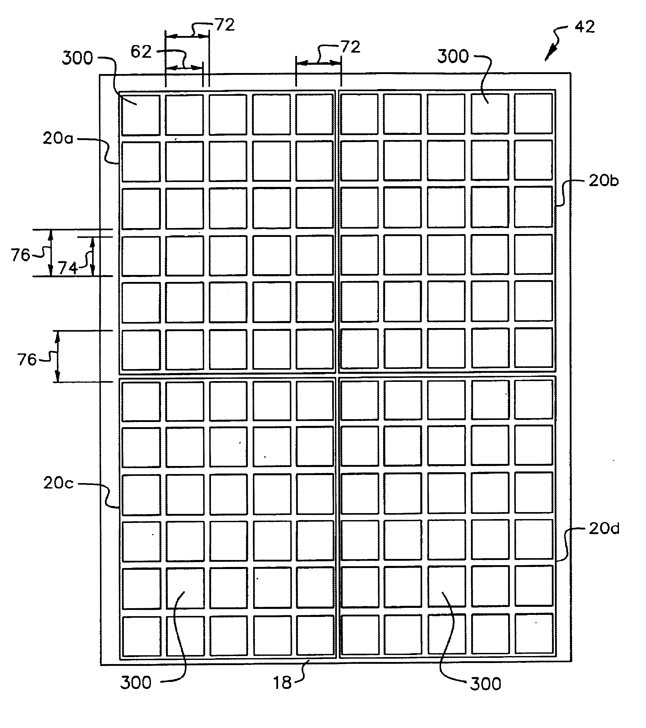
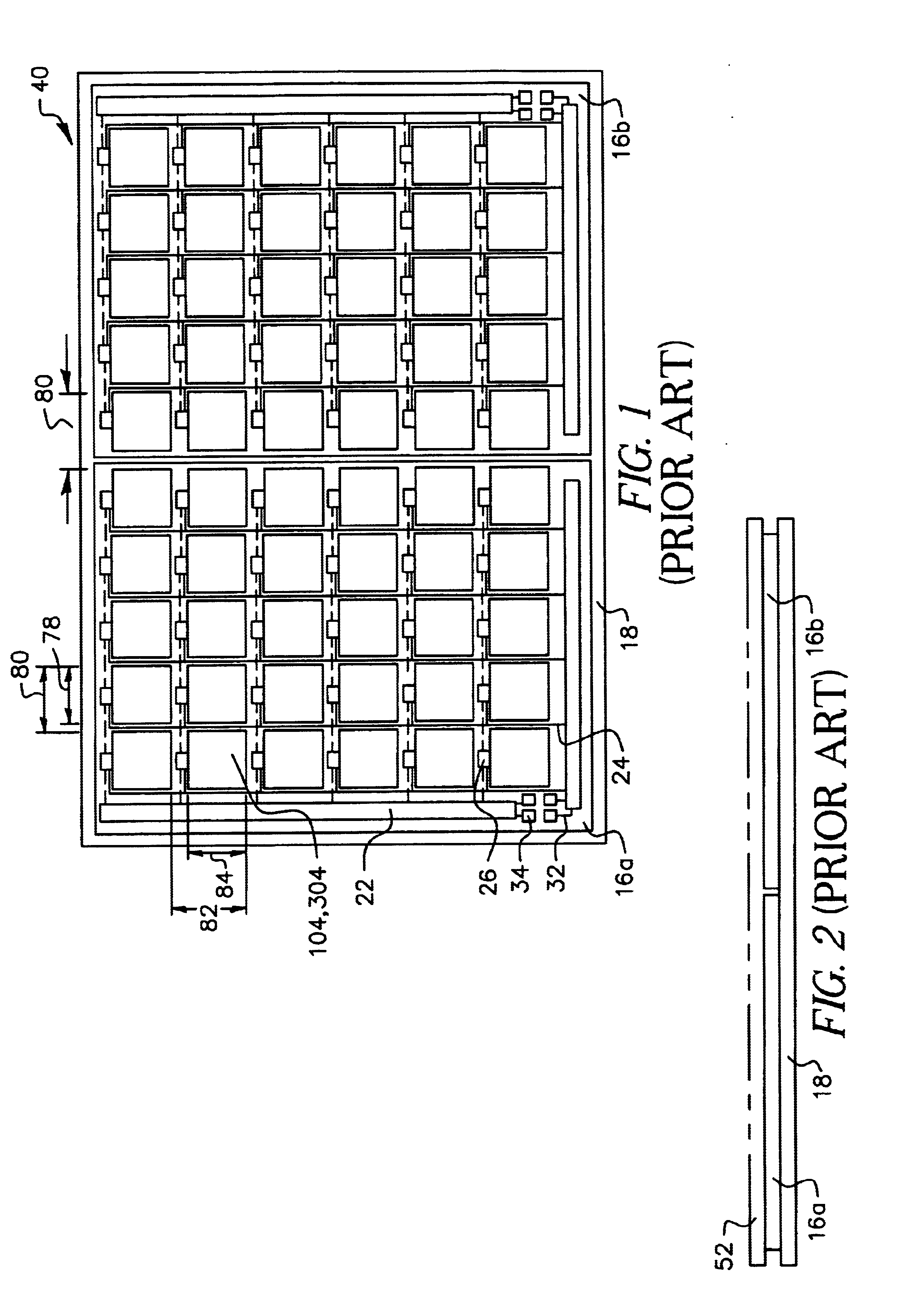
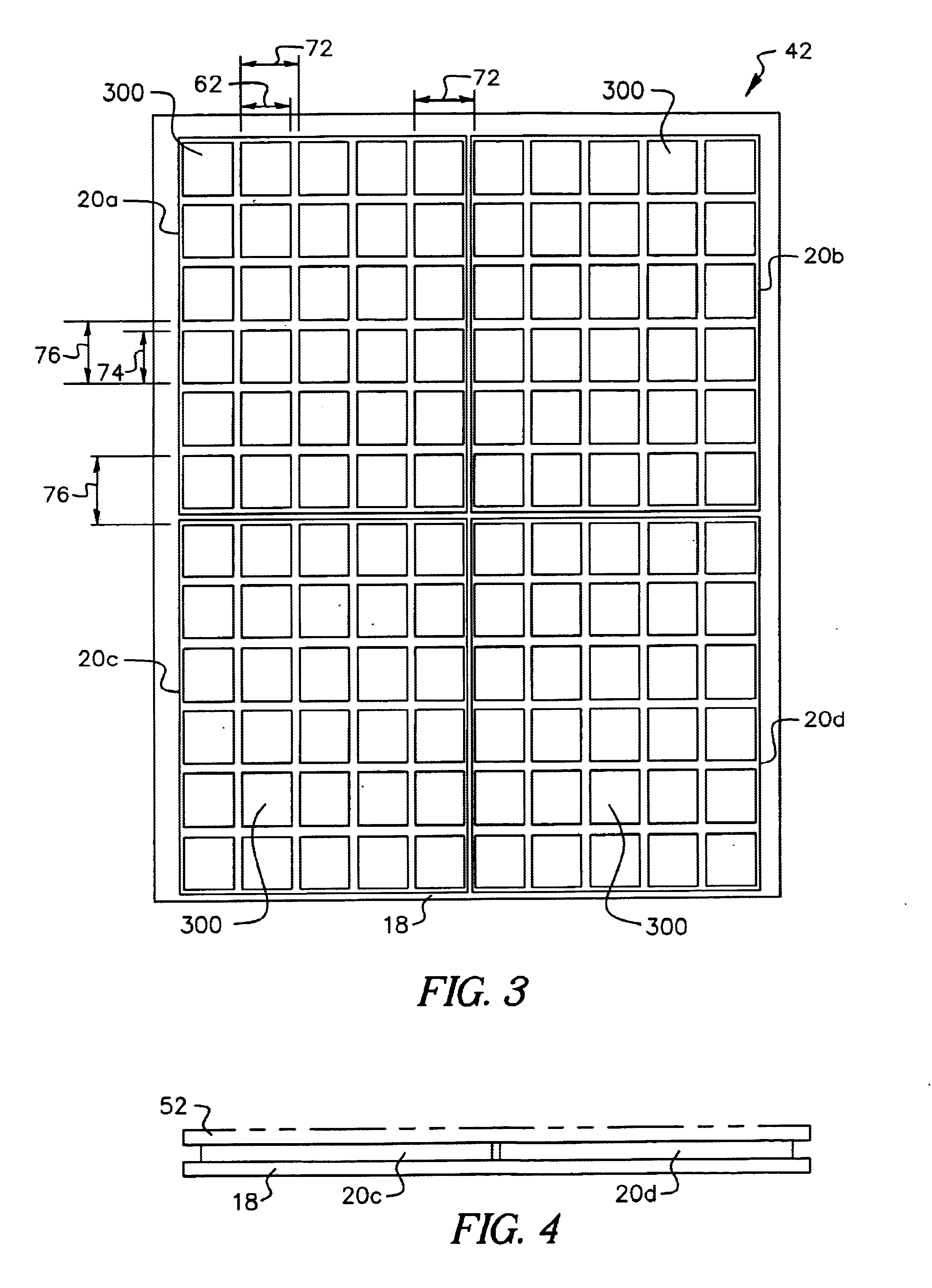
Turning now to FIGS. 1 and 2 which show a prior art for a tiled display 40 having a plurality of tiles 16a-16b each with circuits 26 and drive circuits 22 and pixel electrodes 104 or 304, formed on a back plate 18. It is understood that the drive circuits 22, circuits 26 and pixel electrodes 104 or 304 for each tile 16a-16b exist in the same circuit layer. It is further understood that the circuit 26 includes the thin film transistors and associated capacitors. The pixel aperture ratio is limited by the space required for the circuits 26 and, furthermore, the drive circuits 22 extend beyond the area defined by the outermost pixels on each tile. Alternately, the drive circuits 22 are separate discrete components that are interconnected to the tile using tape automated bonding or other means. The horizontal pitch 80 between adjacent pixels on adjacent tiles, across a seam, is substantially equivalent to the horizontal pixel pitch 80 on a single tile. Additionally, the vertical pixel p...


PUM

PropertyMeasurementUnit
electric fieldaaaaaaaaaa
electricalaaaaaaaaaa
transparentaaaaaaaaaa

Abstract

A high aperture ratio emissive tiled display comprised of a plurality of tiles including a substrate with discrete layers of integrated drive circuits, thin film transistors, circuit conductor layer and light-emitting pixel array wherein all the electronic circuitry is contained under the pixel array. Vertical interconnects are made between the drive circuits, circuits and pixel electrodes, as necessary, and can include vertical interconnections through the substrate. Large flat panel displays including at least two of said tiles are aligned to maintain pixel pitch from one tile to another to produce a seamless image.

Description

FIELD OF THE INVENTIONThe present invention relates to high aperture ratio displays, which include a plurality of tiles aligned to produce an image.BACKGROUND OF THE INVENTIONFlat panel displays are found everywhere from hand held electronics to large scale video applications. Larger displays are usually smaller displays tiled together. When the displays are tiled it is important to create a bright image that appears seamless across the tiles. The image brightness is proportional to the size of the aperture ratio in the display as defined by the ratio of the emissive surface area of a pixel to the total surface area of the same pixel. Increasing the aperture ratio of the pixel produces a brighter image. However, increasing the space between pixels allows for a proportional increase in the spacing between adjacent tiles, thereby facilitating the ability to create a seamless tiled display. Therefore, any increase in the area available for each pixel can be distributed optimally to inc...

Claims


Application Information

Patent Timeline
Patent Type & Authority Patents(United States)
IPC IPC(8): G02F1/13G02F1/1333G09G3/20G09F9/40G02F1/133G06F3/14G09F9/30H01L27/32
CPCG09G3/20H01L27/3293G06F3/1446H01L27/3297H01L27/3244G09G2300/026H10K59/18H10K59/12H10K59/131G02F1/133
Inventor FREIDHOFF, HENRY R.PHELAN, GIANA M.
Owner GLOBAL OLED TECH
Why Eureka
Try Eureka