Flash memory device having uniform threshold voltage distribution and method for verifying same

a flash memory and threshold voltage technology, applied in static storage, digital storage, instruments, etc., can solve the problems of flash memory cells of page units to be incompletely erased in an erase operation, charge fluctuation on the floating gate,

Active Publication Date: 2005-02-08
SAMSUNG ELECTRONICS CO LTD
View PDF2 Cites 55 Cited by
  • Summary
  • Abstract
  • Description
  • Claims
  • Application Information

AI Technical Summary

Benefits of technology

The page buffer includes a first NMOS transistor coupled to the flash memory cells and responsive to a first bitline control signal. A first PMOS transistor is coupled to the first NMOS transistor and capable of precharging a sensing node to a predetermined voltage level responsive to a precharge signal. A second NMOS transistor is coupled to the sensing node and gates to a second bitline control signal. A latch is coupled to the second NMOS transistor and capable of latching the voltage at the sensing node. A third NMOS transistor is coupled to the latch and responsive to the voltage at the sensing node. A fourth NMOS transistor is coupled between the third NMOS transistor and a ground voltage and capable of storing the flash memory cell data in the latch responsive to a first latch control signal. And a fifth NMOS transistor is coupled between the sensing node and a ground voltage and capable of resetting the sensing node responsive to a bitline reset signal.
The page buffer includes a sixth NMOS transistor capable of transferring data inputted in a program operation of the flash memory device responsive to a data loading enable signal. A second latch stores the inputted data. A seventh NMOS transistor is coupled to the secon

Problems solved by technology

Threshold voltage variation results in charge fluctuation on the floating gate.
The non-uniform distribution of the flash memory cells hav

Method used


Image

  • Flash memory device having uniform threshold voltage distribution and method for verifying same
  • Flash memory device having uniform threshold voltage distribution and method for verifying same
  • Flash memory device having uniform threshold voltage distribution and method for verifying same

Examples


Embodiment Construction

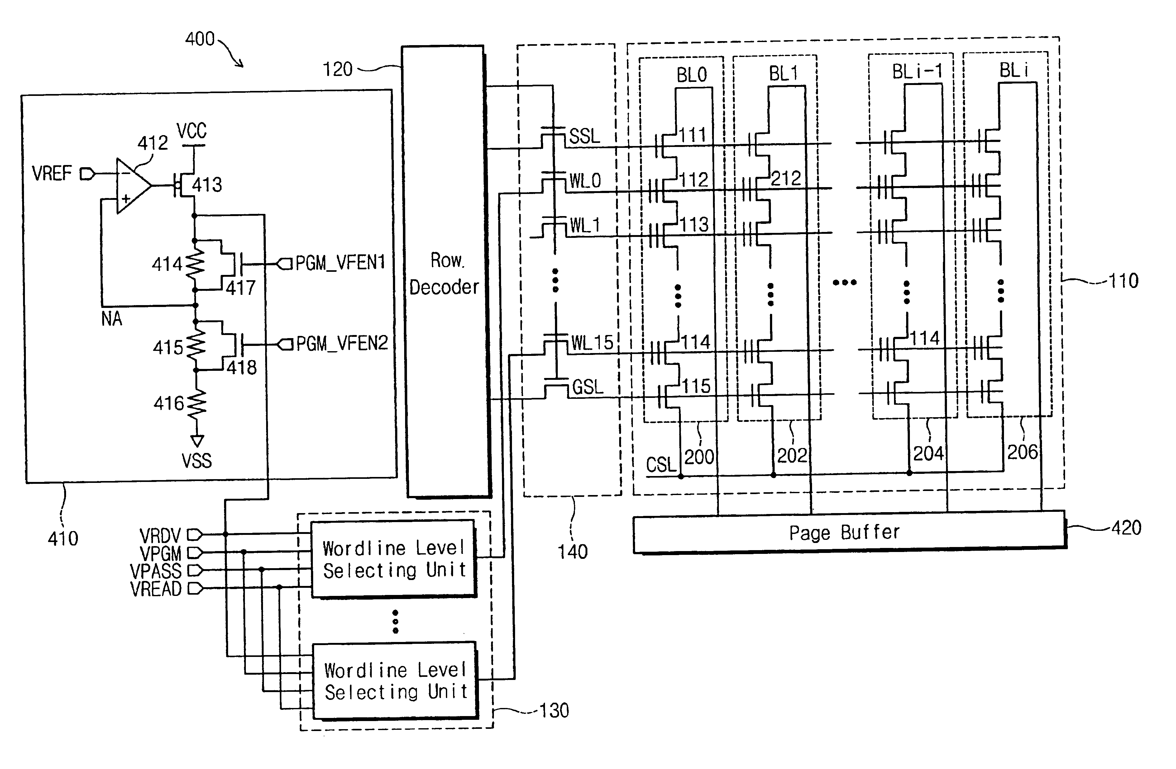
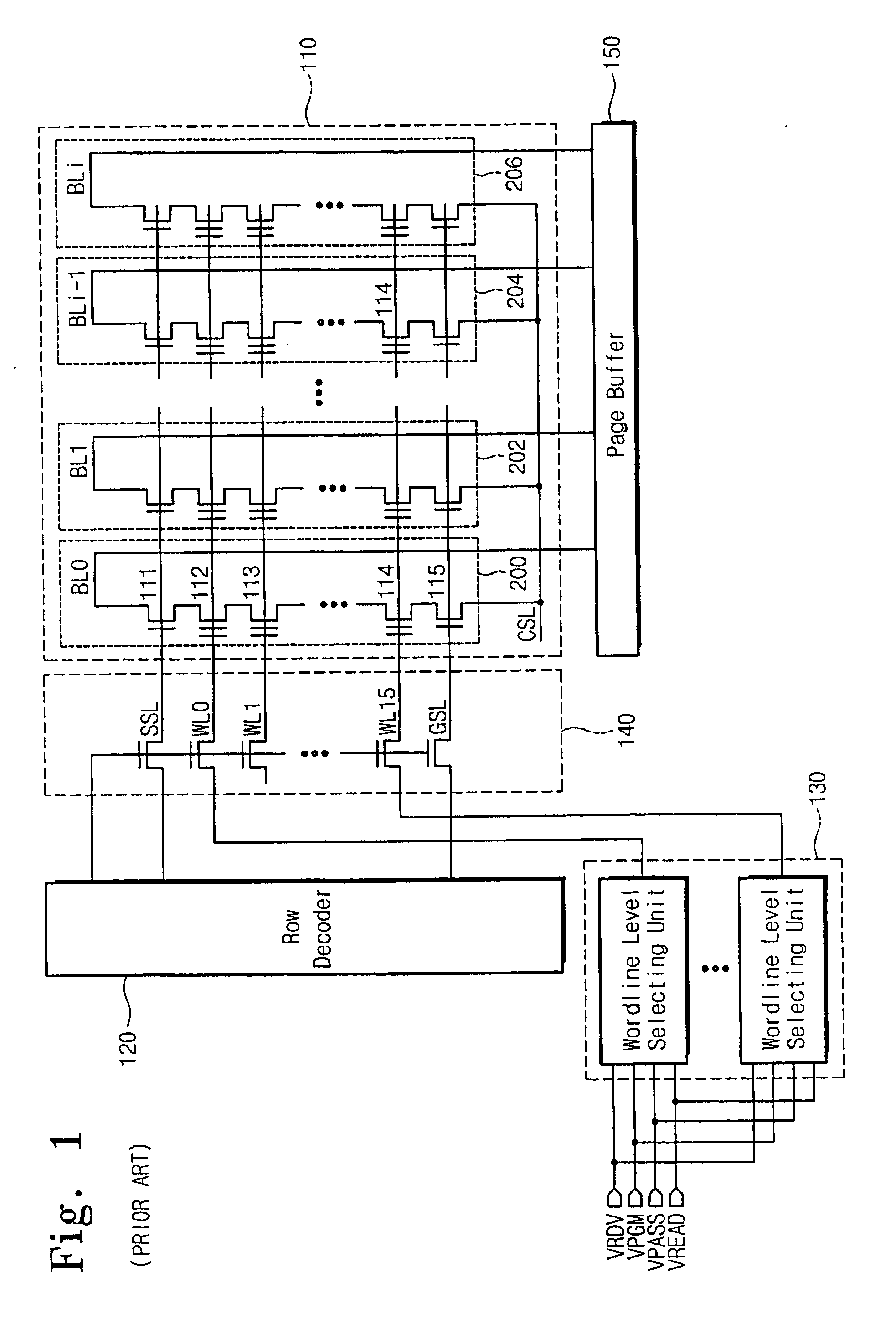
A flash memory device according to the present invention is now described below with reference to FIG. 4. Referring to FIG. 4, a flash memory device 400 includes a memory cell array block 110, a row decoder 120, a wordline level selecting unit 130, a program verify voltage generating unit 410, and a page buffer 420. The memory cell array block 110, the row decoder 120, and the wordline level selecting unit 130 are similar with those described earlier with reference to FIG. 1.

The program verify voltage generating unit 410 has a PMOS transistor 413 and first to third resistors 414, 415, and 416 that are serially coupled between a power supply voltage VCC and a ground voltage VSS. Further, the program verify voltage generating unit 410 has a first NMOS transistor 417 coupled to both ends of the first resistor 414 and a second NMOS transistor 418 coupled to both ends of the second resistor 415. The PMOS transistor 412 gates to an output of a comparator 412 for comparing a reference volt...


PUM


Abstract

A flash memory device including a memory cell array block including a plurality of flash memory cells. A program verify voltage generating unit variably generates a program verify voltage that verifies flash memory cells programming. A wordline level selecting unit transfers the program verify voltage to the flash memory cells. And a page buffer, including a latch, stores flash memory cell data and resets the latch whenever the program verify voltage is lowered.

Description

CROSS REFERENCE TO RELATED APPLICATIONSThis application claims priority from Korean Patent Application No. 2002-76955, filed on Dec. 5, 2002, the contents of which are incorporated herein by reference in their entirety.FIELD OF THE INVENTIONThe present invention relates to a semiconductor memory device and, more particularly, to a flash memory device having a uniform threshold voltage distribution without misprogrammed cells.BACKGROUND OF THE INVENTIONA flash memory device is a highly integrated information storage device in which write and erase operations are accomplished on board. A flash memory cell includes at least one field effect transistor (FET) having a selection gate, a floating gate, a source, and a drain. Threshold voltage variation results in charge fluctuation on the floating gate. The charge fluctuation is data that is stored in the flash memory cell.Flash memory devices are classified into NAND and NOR devices. The NAND flash memory device is used as a mass data sto...

Claims


Application Information

Patent Timeline
IPC IPC(8): G11C16/02G11C11/34G11C16/06G11C16/04G11C16/12G11C16/34
CPCG11C16/3459G11C16/3454G11C16/0483G11C2216/14G11C16/12
Inventor LEE, KYEONG-HANLEE, SUNG-SOO
Owner SAMSUNG ELECTRONICS CO LTD
Why Eureka
Try Eureka