Castellation wafer level packaging of integrated circuit chips

a castellation wafer and integrated circuit technology, applied in the direction of electrical equipment, semiconductor devices, semiconductor/solid-state device details, etc., can solve the problems of many steps required for etching and connecting, many steps required for deposited materials for conduction and insulation, and many known techniques, etc., to achieve the effect of reliable electrical characteristics of trace lines

Inactive Publication Date: 2005-02-15
MICRON TECH INC
View PDF5 Cites 98 Cited by
  • Summary
  • Abstract
  • Description
  • Claims
  • Application Information

AI Technical Summary

Benefits of technology

Once the chips are deposited on the second wafer, an encapsulant is deposited. The encapsulant is deposited such that the top surface of the encapsulant is level with the faces of the chips and preferably slightly below the level of the faces of the castellation blocks. The encapsulant is deposited to hold the castellation blocks in place. After the encapsulant is deposited, a passivation layer is deposited over the chips and the encapsulant (the chip pads of the active circuits are preferably left exposed or are exposed in a subsequent step of the fabrication process). Metal trace lines are deposited from the castellation blocks to the chip pads of the active circuits. The passivation layer is preferably substantially even with the level of the faces of the castellation blocks such that the electrical characteristics of the trace lines are more reliable.

Problems solved by technology

These known techniques, however, have several drawbacks.
One such drawback is the many steps required for depositing layers of materials for conduction and insulation.
These techniques also require many steps for etching and connecting leads.
These internal leads are more susceptible to breaking or otherwise malfunctioning than larger, more rigid contacts that can be easily coupled to the active circuit areas via, for example, a trace line.
In other words, these castellation contacts used with these known techniques are often mechanically unsound and not sturdy (e.g., they may move and break), thus causing undesired electrical discontinuities.
Because only one package is fabricated at a time and each requires many steps of depositing and etching, the cost and time to fabricate a package is high.
Moreover, because only one package is fabricated at a time, the amount of materials used to fabricate the package is not used efficiently.
The known techniques waste much of the materials used that could otherwise be used to fabricate multiple packages in the same process.
Another drawback of the known techniques is that the chips included in the packages are not well protected.
In those cases where a protective material is incorporated into the package, that protective material is often suspended above the chip, which limits the protection.

Method used


Image

  • Castellation wafer level packaging of integrated circuit chips
  • Castellation wafer level packaging of integrated circuit chips
  • Castellation wafer level packaging of integrated circuit chips

Examples


Embodiment Construction

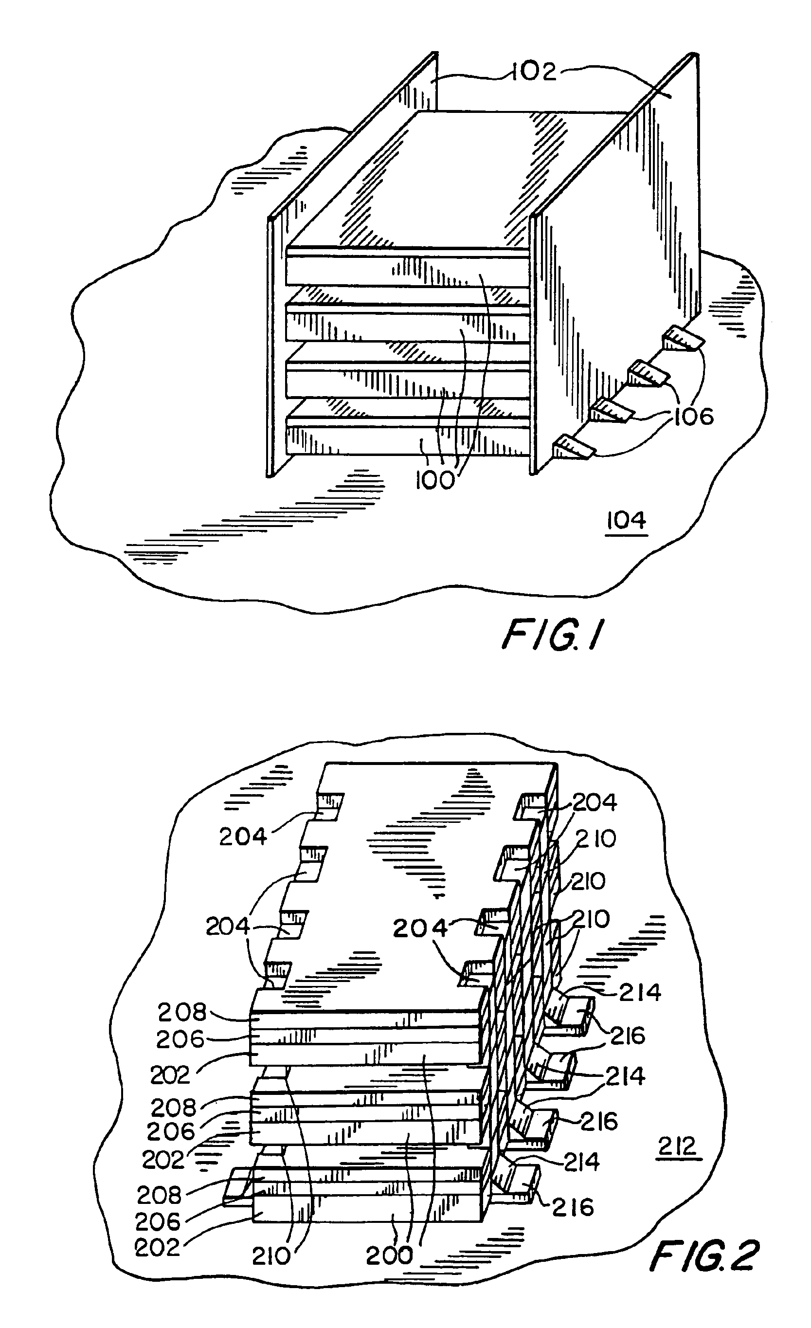
FIGS. 1 and 2 illustrate preferred packages fabricated in accordance with the invention. In the embodiment shown in FIG. 1, packages 100 are stacked on top of one another. Contacts at the edge of the packages 100 (not shown) are soldered to printed circuit boards (PCB) 102. The contacts are coupled to the active circuit areas of integrated circuit chips in packages 100. Printed on PCBs 102 are conductors (not shown) coupling the respective contacts of each package 100. The contacts of packages 100 are also coupled to, for example, motherboard 104 by solder 106 which is coupled to the conductors printed on PCBs 102.

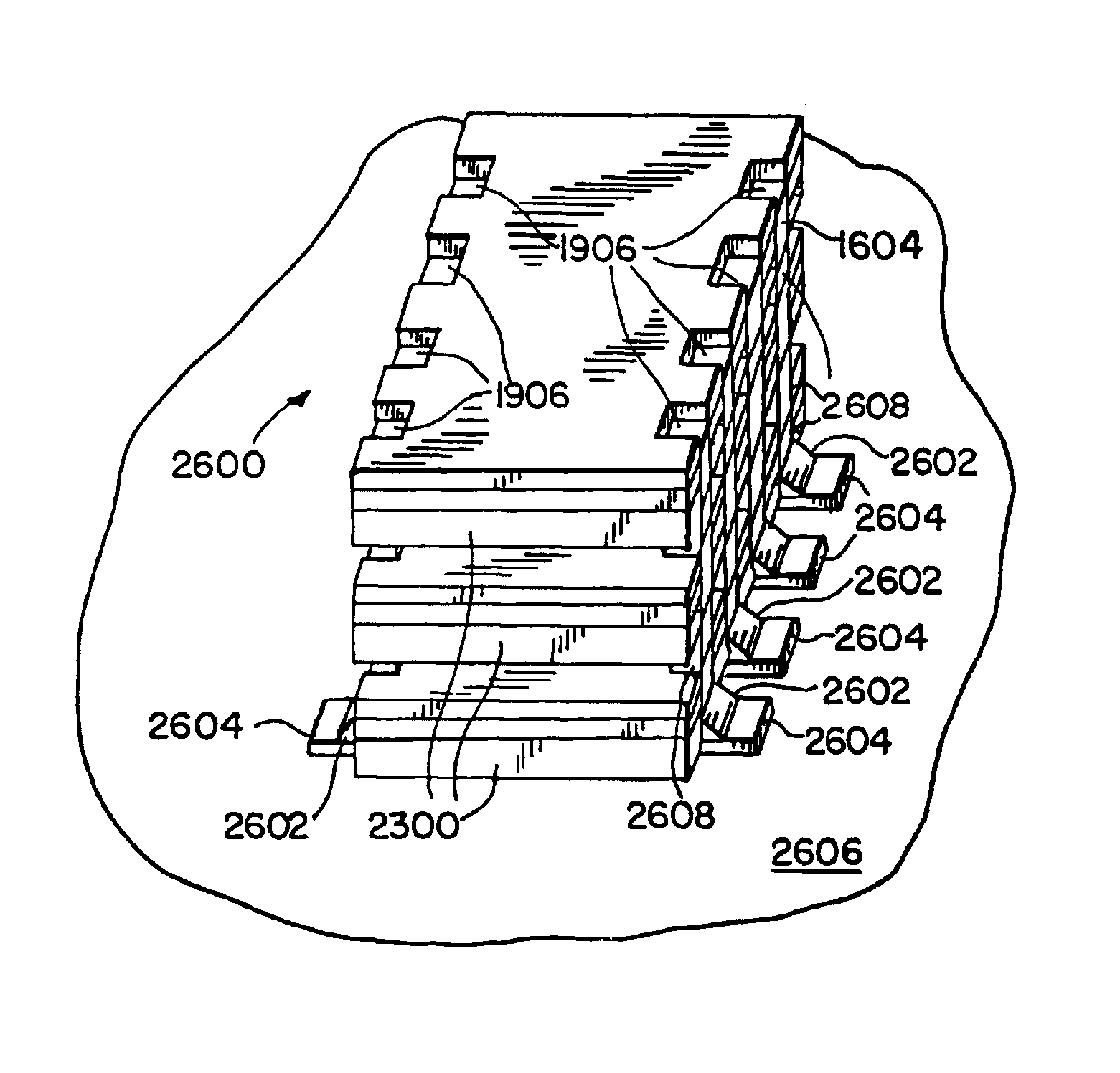
In the embodiment shown in FIG. 2, packages 200 are also stacked on top of one another. Each package 200 includes an integrated circuit chip (not shown) encapsulated by an encapsulant 202. Encapsulant 202 holds contacts 204 in place. Contacts 204 are coupled to the active circuit areas of the integrated circuit chip by conductors. Passivation interlayers 206 are deposited ...


PUM


Abstract

Systems and methods for packaging integrated circuit chips in castellation wafer level packaging are provided. The active circuit areas of the chips are coupled to castellation blocks and, depending on the embodiment, input/output pads. The castellation blocks and input/output pads are encapsulated and held in place by an encapsulant. When the devices are being fabricated, the castellation blocks and input/output pads are sawed through. If necessary, the wafer portion on which the devices are fabricated may be thinned. The packages may be used as a leadless chip carrier package or may be stacked on top of one another. When stacked, the respective contacts of the packages are preferably coupled. Data may be written to, and received from, packaged chips when a chip is activated. Chips may be activated by applying the appropriate signal or signals to the appropriate contact or contacts.

Description

BACKGROUND OF THE INVENTIONThis invention relates to systems and methods for packaging integrated circuit chips in castellation wafer level packaging. More particularly, this invention relates to castellation wafer level packaging that can be stacked on top of one another and alternatively can be used individually as leadless chip carriers.Castellation wafer level packaging includes techniques for packaging chips in packaging slightly larger than the chips. The externally accessible contacts to the chips are the surfaces of solid blocks of conductive material. The solid blocks, referred to as castellation blocks or contacts, have notable length, width, and height dimensions relative to the packaging.Techniques for packaging integrated circuit chips in packages that include castellation contacts are known. Such techniques include packaging chips in leadless chip carriers. These carriers can be easily placed into and taken out of devices that receive such carriers. Leadless chip carri...

Claims


Application Information

Patent Timeline
Patent Type & Authority Patents(United States)
IPC IPC(8): H01L21/02H01L21/50H01L23/02H01L21/44H01L23/31H01L23/485H01L25/10
CPCH01L23/3114H01L24/18H01L25/105H01L25/50H01L24/05H01L2924/1461H01L2224/05624H01L2224/05647H01L2224/18H01L2224/85399H01L2225/06551H01L2924/01005H01L2924/01006H01L2924/01013H01L2924/01014H01L2924/01029H01L2924/0105H01L2924/01079H01L2924/01082H01L2924/014H01L2924/05042H01L2924/14H01L2924/30105H01L23/49805H01L2225/107H01L2225/1035H01L2924/01033H01L2924/00014H01L2224/45099H01L2924/00H01L2924/181H01L2924/12042H01L2224/02371H01L2224/04105H01L2224/73267H01L2924/18162H01L24/24
Inventor JEUNG, BOON SUANPOO, CHIA YONGWAF, LOW SIUKOON, ENG MEOWKWANG, CHUA SWEEWU, HUANG SHUANGLOO, NEO YONGWEI, ZHOU
Owner MICRON TECH INC
Why Eureka
Try Eureka