Method for conductance switching in molecular electronic junctions

a technology of electronic junctions and conductance switching, which is applied in the direction of thermoelectric devices, solid-state devices, and nano-informatics. it can solve the problems of inability to meet the chemical requirements of a successful molecular switch, the inability to know the switch mechanism in most cases, and the formidable hurdles of practical utility

Inactive Publication Date: 2005-02-15
THE OHIO STATES UNIV
View PDF8 Cites 50 Cited by
  • Summary
  • Abstract
  • Description
  • Claims
  • Application Information

AI Technical Summary

Benefits of technology

[0019]Compatibility with conventional

Problems solved by technology

Although several examples of conductance switching have been extensively investigated, the switching mechanism in most cases is unknown, and the subject of some controversy.
The mechanism is controversial and the chemical requirements for a successful molecular switch are unknown.
Single molecule or nanoscale electronic devices hold exceptional promise for technical and economic value, but also present formidable hurdles for practical utility, and massively parallel fabrication.
Although the gold/thiol and Langmuir-Blodgett structures used to fabricate these molecular devices have been widely studied, they have yet to yield a commercial electronic product.
First, the Au/thiol SAM is widely studied and relatively simple to prepare, but is pron

Method used


Image

  • Method for conductance switching in molecular electronic junctions
  • Method for conductance switching in molecular electronic junctions
  • Method for conductance switching in molecular electronic junctions

Examples


Embodiment Construction

)

[0078]In accordance with the forgoing summary, the following presents a detailed description of the preferred embodiment of the invention that is currently considered to be the best mode.

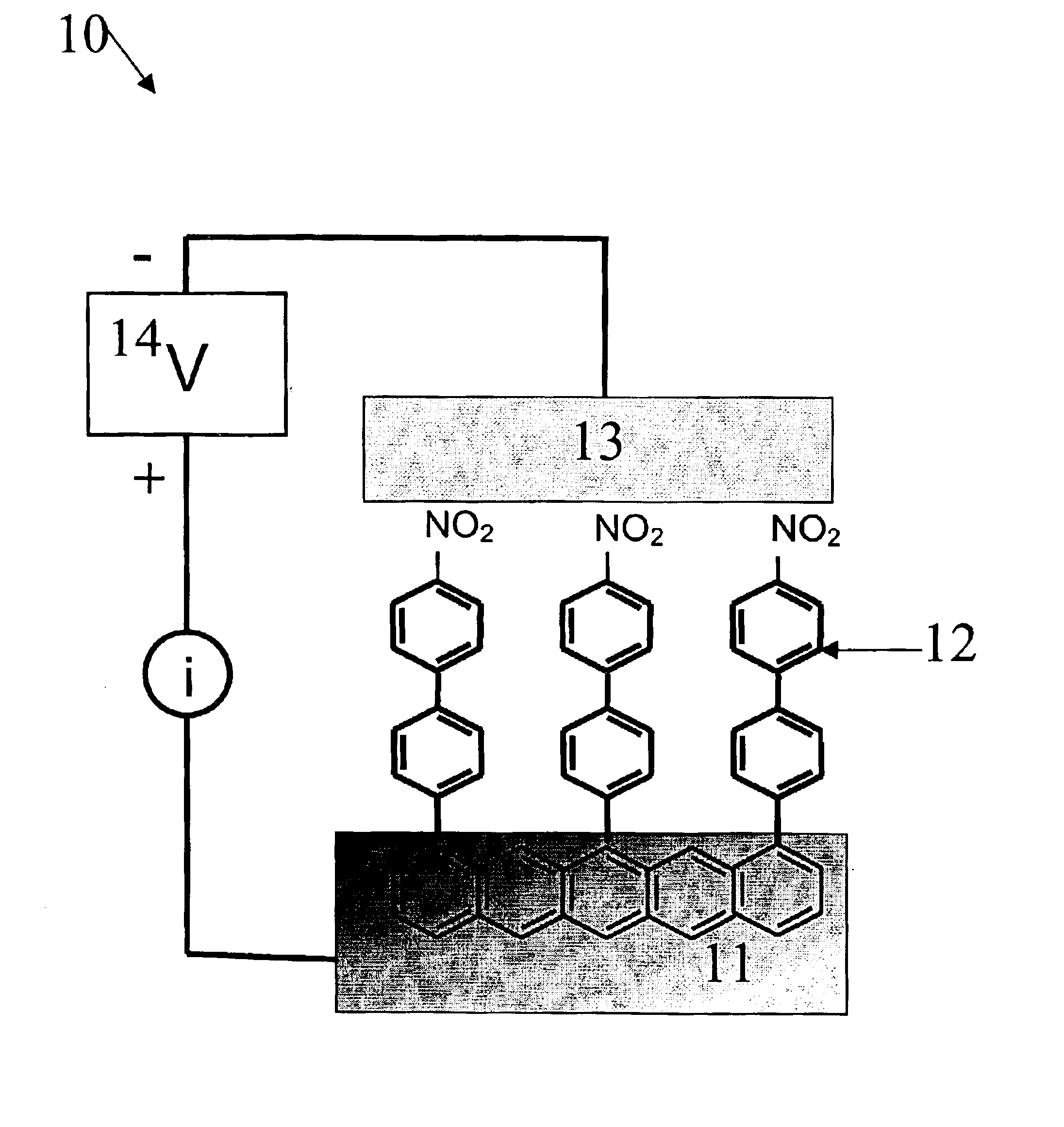
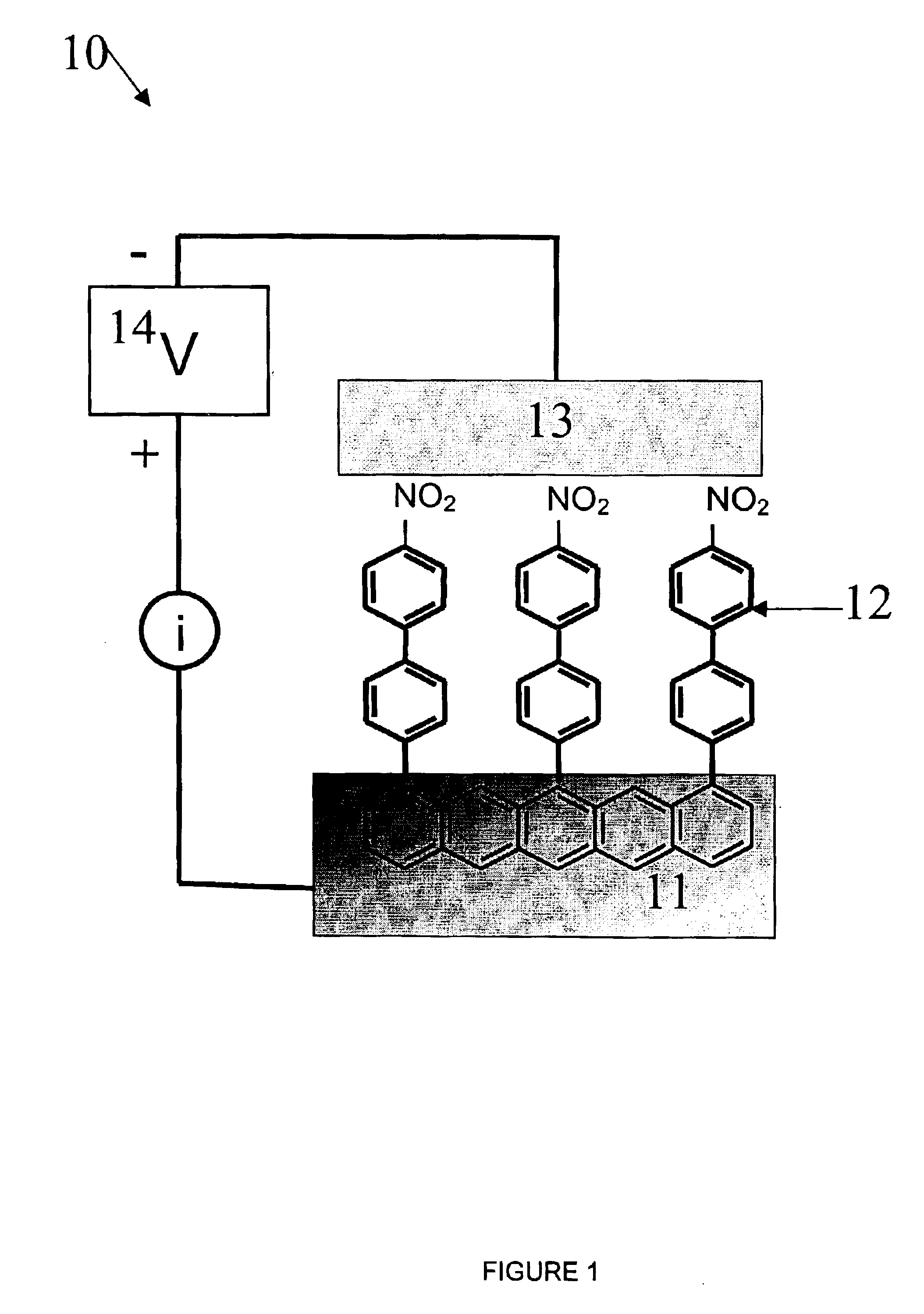
[0079]Our approach is much simpler than the alternatives. Specifically, a molecule in our junctions is induced to “switch” by molecular rearrangement in response to a high electric field. Molecules such as nitroazobenzene, nitrobiphenyl, terphenyl, and diethylaminophenyl are aromatic when bonded to a carbon (and / or metal or silicon) surface, and the rings are generally twisted with respect to each other and the carbon substrate. In a high static electric field, these molecules rearrange to a quinoid structure, in a process analogous to a redox reaction, but without counterions or solvent. The quinoid structure is more conjugated than the original molecule, as judged by changes in bond length and increased polarizability. Stronger electronic coupling or orbitals across the quinoid structure presumab...


PUM


Abstract

The present invention includes a chemical monolayer construction that comprises: a substrate having a contact surface, and a monolayer of a plurality of substantially parallel molecular units attached to the contact surface of the substrate. The molecular units are strongly coupled electronically to the substrate. The contact surface of the substrate has a roughness value less than or equal to the average length of the molecular units. The molecular units comprise a chemical structure that is capable of being changed from a relatively non-conductive state to a relatively conductive state by the application of a stimulus. The present invention also includes electronic circuit components and devices including chemical monolayer constructions.

Description

[0002]The present application claims priority to U.S. provisional application No. 60 / 365,465, filed Mar. 19, 2002 and to U.S. provisional application No. 60 / 405,397, filed Aug. 23, 2002, both of which are hereby incorporated in their entirety by reference.[0003]The present invention was made with Government support under Grant No. RF 737159 awarded by the National Science Foundation. The United States Government may have certain rights to this invention under 35 U.S.C. §200 et seq.TECHNICAL FIELD OF THE INVENTION[0004]The present invention is in the field of chemical monolayers and microelectronic junctions, and includes chemical sensors, photosensors, electrochemical devices, memory devices, and other devices containing them.BACKGROUND OF THE INVENTION[0005]Conductance switching is the basis of many potential molecular electronic devices, and has been the focus of numerous research efforts in recent years. If a single molecule or an assembly of molecules can be switched between a h...

Claims


Application Information

Patent Timeline
IPC IPC(8): H01L51/30H01L51/05H01L51/00
CPCB82Y10/00H01L51/0595H01L51/0051H10K85/611H10K10/701
Inventor MCCREERY, RICHARD L.
Owner THE OHIO STATES UNIV
Why Eureka
Try Eureka