Semiconductor memory and method of driving the same

a technology of semiconductors and memory, applied in the direction of transistors, digital storage, instruments, etc., can solve the problems of deteriorating the data holding characteristic of the memory, unable to obtain satisfactory data holding characteristics of the memory, etc., and achieve the effect of shortening the time produced in the data erase sequen

Inactive Publication Date: 2005-02-15
MONTEREY RES LLC
View PDF2 Cites 17 Cited by
  • Summary
  • Abstract
  • Description
  • Claims
  • Application Information

AI Technical Summary

Benefits of technology

In this configuration, data can be erased after electrons trapped in the first gate insulating film...

Problems solved by technology

Accordingly, no satisfactory data holding characteristic of the memory can...

Method used


Image

  • Semiconductor memory and method of driving the same
  • Semiconductor memory and method of driving the same
  • Semiconductor memory and method of driving the same

Examples


first embodiment

(First Embodiment)

A semiconductor memory and method of driving the same according to the first embodiment of the present invention will be described below with reference to the accompanying drawings. This embodiment will be explained by taking a NOR memory cell as an example of the memory cell of the semiconductor memory.

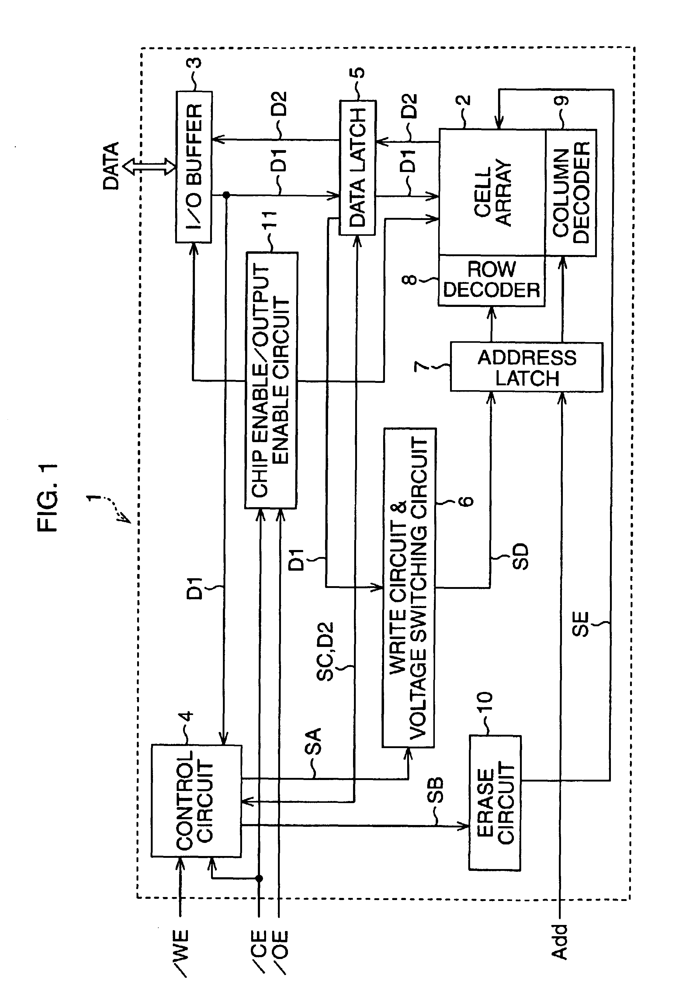
FIG. 1 is a block diagram showing an example of the arrangement of the semiconductor memory according to this embodiment.

Referring to FIG. 1, a semiconductor memory 1 includes a cell array 2, an I / O buffer 3, a control circuit 4, a data latch 5, a write circuit & voltage switching circuit 6, an address latch 7, a first decoder 8, a second decoder 9, an erase circuit 10, and a chip enable / output enable circuit 11.

The cell array 2 has a plurality of memory cells which primarily store data supplied from an external device (not shown).

As described above, this embodiment uses a NOR structure memory cell array in which a plurality of memory cells are connected in parallel...

second embodiment

(Second Embodiment)

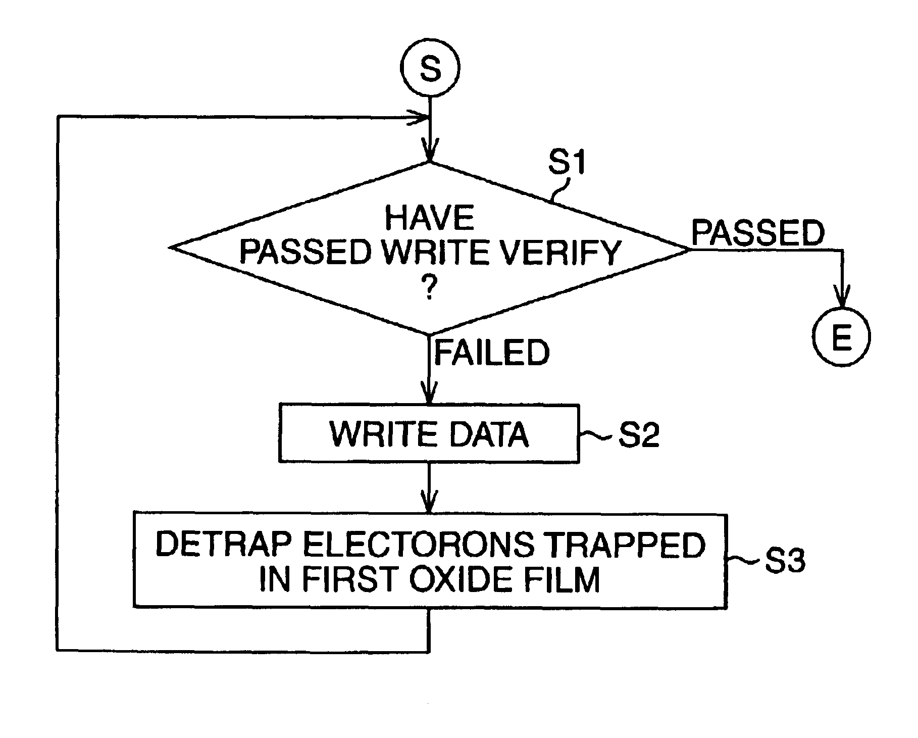
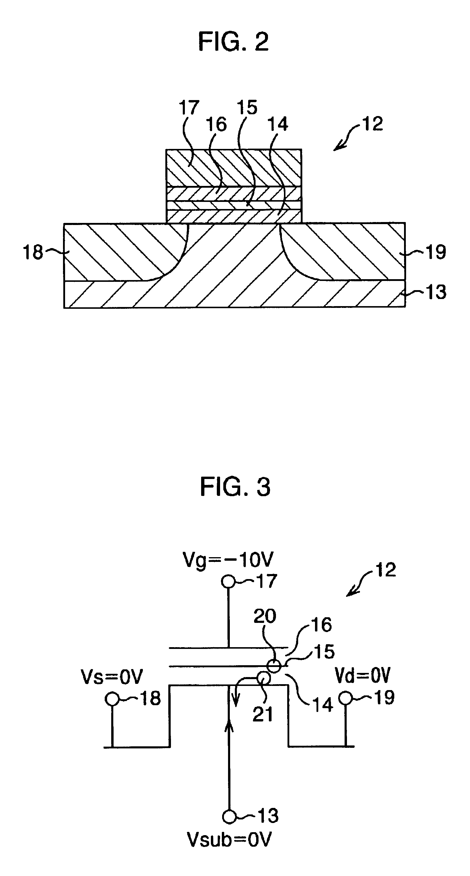
A semiconductor memory and method of driving the same according to the second embodiment of the present invention will be described below. This embodiment is the same as the aforementioned first embodiment except for a sequence of detrapping electrons 21 trapped in a first gate oxide film 14 into a p-type silicon substrate 13 during a data erase operation. Hence, the same reference numerals as in the first embodiment denote the same parts, and a detailed description thereof will be omitted.

The data erase sequence of the semiconductor memory of this embodiment will be explained with reference to a flow chart in FIG. 8.

First, in steps S21 to S24, a write-before-erase sequence is executed in the same manner as in steps S11, S12, S14, and S15 of FIG. 6 explained in the first embodiment described above.

That is, if determining in step S21 by write verify that data is not written in all bits at addresses in a sector from which data is to be erased, a control circuit 4 ge...


PUM


Abstract

Immediately after data write, a negative voltage which has an absolute value lager than that in data erase and which falls within a range over which no FN current flows is applied to a control gate, and at the same time 0 V is applied to a silicon substrate, source, and drain. In this manner, electrons trapped in a first gate oxide film are detrapped into the silicon substrate. This prevents a memory cell from passing write verify although electrons stored in a nitride film are few, prevents data changes caused by a decrease in the read margin, and improves the data holding characteristic of a memory cell.

Description

CROSS-REFERENCE TO RELATED APPLICATIONSThis application is based upon and claims priority of Japanese Patent Application No. 2001-367052, filed on Nov. 30, 2001, the contents being incorporated herein by reference.BACKGROUND OF THE INVENTION1. Field of the InventionThe present invention relates to a semiconductor memory and method of driving the same and, more particularly, to a semiconductor memory and method of driving the same suitable for use in data rewrite.2. Description of the Related ArtA flash memory is a nonvolatile memory which holds data by storing electrons into a nitride film formed between gate oxide films. This flash memory has the advantages that, e.g., the fabrication cost can be reduced because the cell structure is simple.Conventional data write and erase operations in a NOR flash memory cell which holds data by storing electrons into a nitride film will be briefly explained below with reference to a sectional view of FIG. 9 which shows an example of the structur...

Claims


Application Information

Patent Timeline
IPC IPC(8): G11C16/04G11C16/02H01L21/8247H01L27/115H01L29/788H01L29/792
CPCG11C16/0466G11C16/3459G11C16/3445
Inventor TAKAHASHI, SATOSHI
Owner MONTEREY RES LLC
Why Eureka
Try Eureka