
Redundancy in series grouped memory architecture

a memory architecture and series grouped technology, applied in the field of memory integrated circuits, can solve the problems of increasing the probability of a failure in the redundant element itself, requiring the replacement of the whole block, and inefficient chained architecture redundancy schemes that use significant chip area, so as to achieve the effect of improving the redundancy schem

Inactive Publication Date: 2005-02-15
POLARIS INNOVATIONS
View PDF7 Cites 4 Cited by
  • Summary
  • Abstract
  • Description
  • Claims
  • Application Information

AI Technical Summary

Benefits of technology

The invention relates to improved redundancy schemes in chained memory architectures. In one embodiment, a memory chain includes x number of first memory cells, where x is equal to or greater than 2 and m second memory cells, where m is equal to or greater than 1. The first memory cells are used for storage of information and the second mem

Problems solved by technology

This means that repairing a defective cell in a block requires replacement of the whole block.
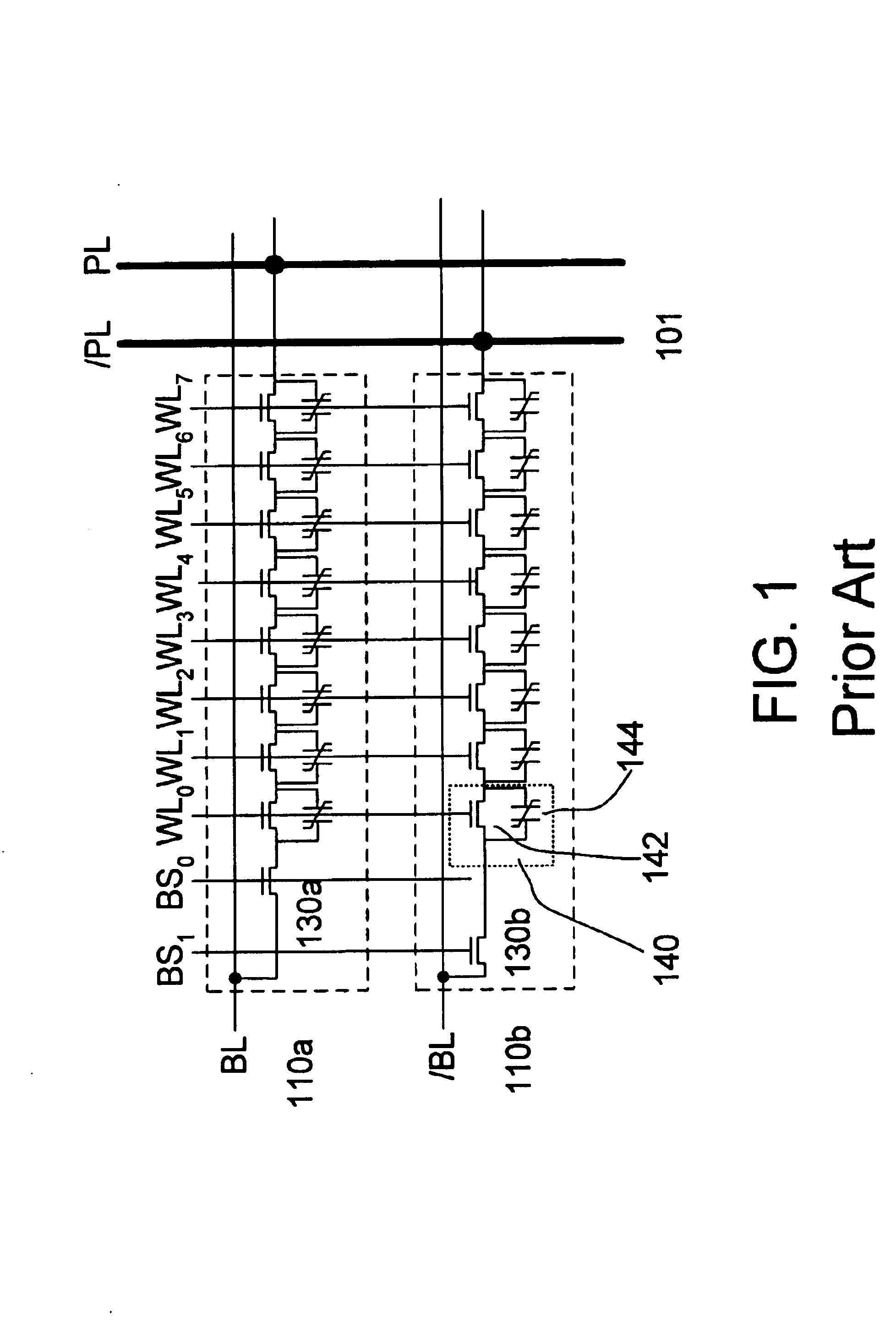
Thus, conventional redundancy schemes in chained architecture are very inefficient and utilize significant chip area.
Additionally, the relatively large number of cells in a redundant element increases the probability of a failure in the redundant element itself.

Method used


Image

  • Redundancy in series grouped memory architecture
  • Redundancy in series grouped memory architecture
  • Redundancy in series grouped memory architecture

Examples


Embodiment Construction

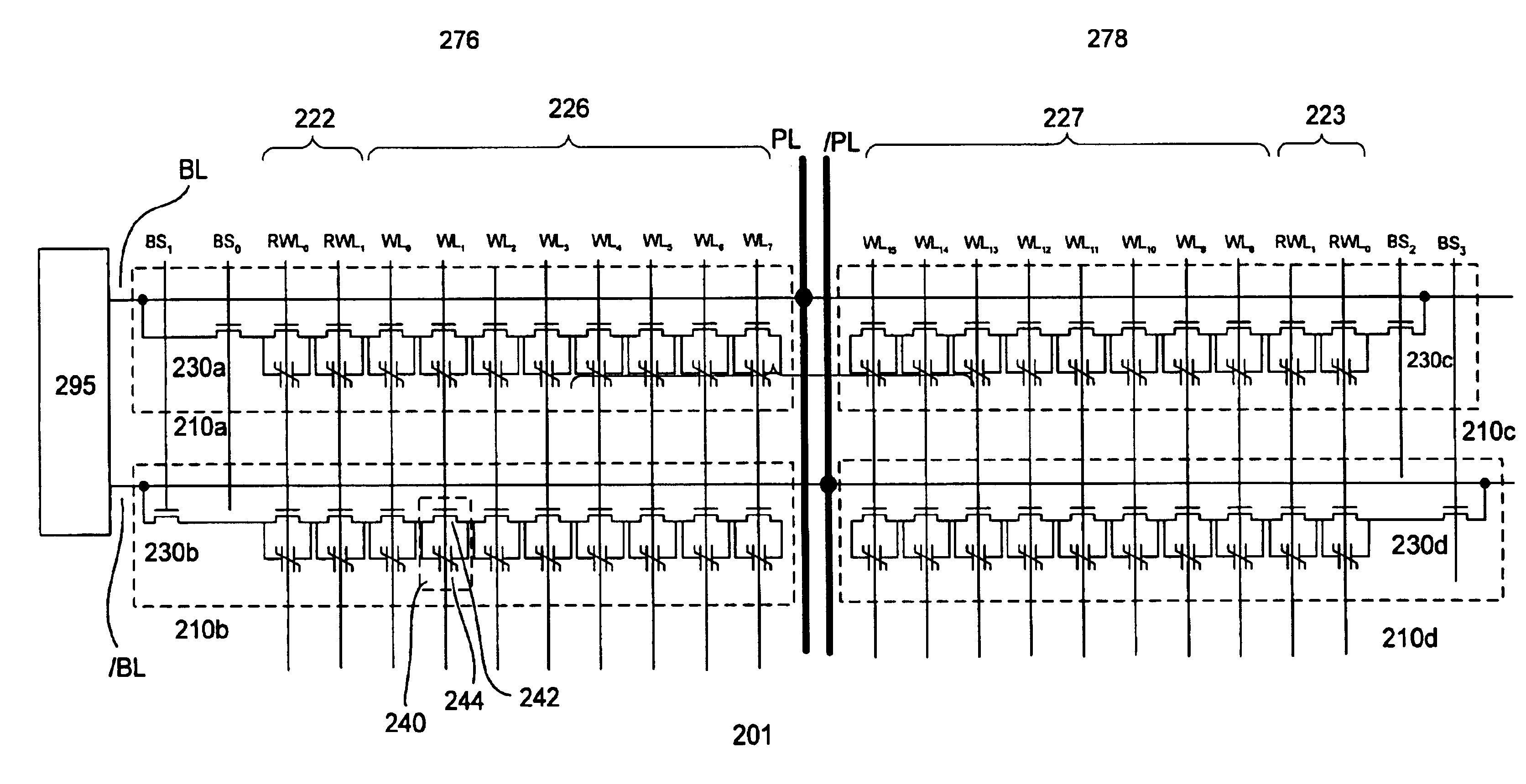
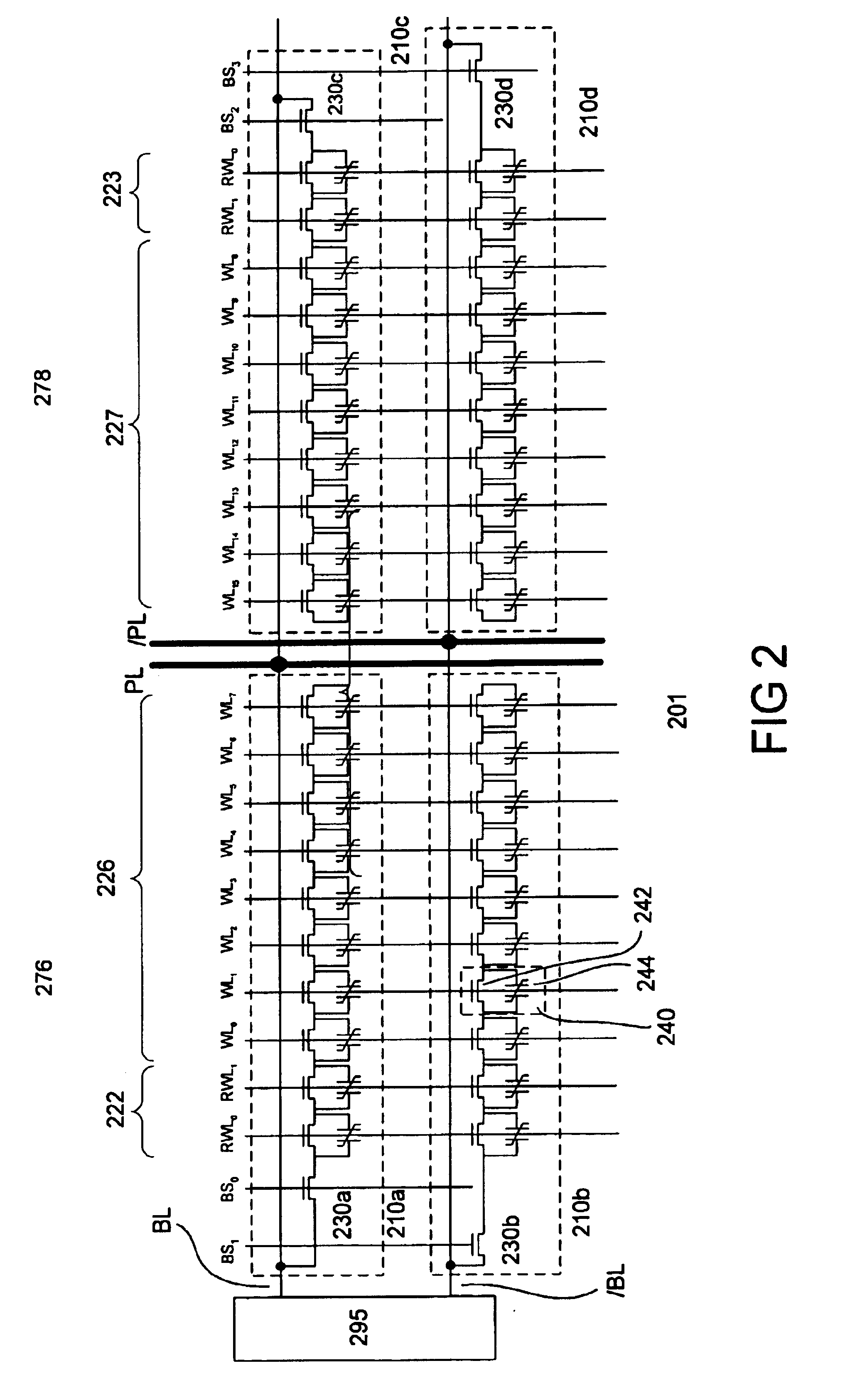
FIG. 2 shows a portion 201 of an IC with redundancy in accordance with one embodiment of the invention. A pair of bitlines (BL and / BL) which represents a column is shown. A plurality of columns are interconnected by wordlines to form a memory block or array. A sense amplifier 295 is coupled to one end of the bitlines. The bitlines each includes a memory chain (210a or 210b). The memory cells 240 of a chain, each with a transistor 242 coupled to a capacitor 244 in parallel, are coupled in series. The memory chain comprises X number of cells 226, where X is a whole number. For practical reasons, X is at least 2. Illustratively, a chain comprises 8 memory cells. Memory chains of other sizes are also useful. Preferably, the memory chain comprises 2y memory cells, where y is ≧1. The gates of the cell transistors can be gate conductors which are coupled to or serve as wordlines. The memory cells are addressed by wordlines WL0-WLx−1.

A selection transistor 230 is provided to selectively co...


PUM


Abstract

An improved redundancy scheme for chained memory architecture is disclosed. The redundancy scheme comprises including redundant cells as part of the memory chain. As such, a redundant cell is used to repair a defective cell within the chain. This eliminates the need in conventional chained architecture to replace the whole memory block when there is a defective cell.

Description

FIELD OF THE INVENTIONThe present invention relates to memory integrated circuits (ICs). More particularly, the invention relates to implementation of redundancy in a chained memory architecture.BACKGROUND OF THE INVENTIONFerroelectric metal oxide ceramic materials such as lead zirconate titanate (PZT) have been investigated for use in ferroelectric semiconductor memory devices. Other ferroelectric materials, for example, strontium bismuth tantalum (SBT) can also be used. The ferroelectric material is located between two electrodes to form a ferroelectric capacitor for storage of information. A ferroelectric capacitor uses the hysteresis polarization characteristic of the ferroelectric material for storing information. The logic value stored in the memory cell depends on the polarization direction of the ferroelectric capacitor. To change the polarization direction of the capacitor, a voltage which is greater than the switching voltage (coercive voltage) needs to be applied across i...

Claims


Application Information

Patent Timeline
IPC IPC(8): G11C29/00G11C11/22G11C29/04
CPCG11C29/816G11C11/22G11C7/00G11C29/00
Inventor REHM, NORBERTJOACHIM, HANS-OLIVERROEHR, THOMASWOHLFAHRT, JOERG W.
Owner POLARIS INNOVATIONS
Learn More