Formable bright film having discontinuous metallic layers
a bright film, discontinuous technology, applied in the field of bright film technology, can solve the problems of introducing human health hazards, prolonging the processing time (and hence costs) associated with metallizing three-dimensional articles, and disadvantageous depositing of metal directly onto articles after the article has been formed, and achieves superior optical and deformation properties
- Summary
- Abstract
- Description
- Claims
- Application Information
AI Technical Summary
Benefits of technology
Problems solved by technology
Method used
Image
Examples
example 1
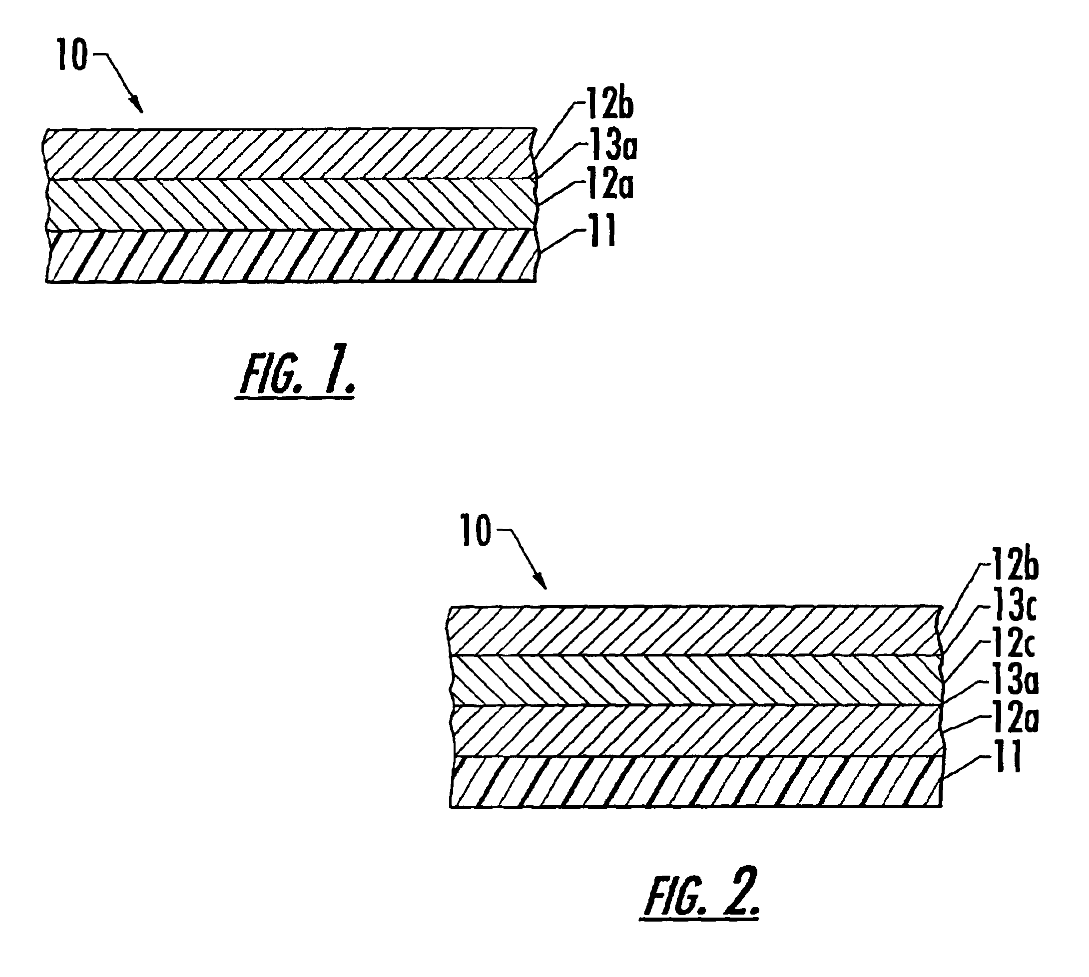
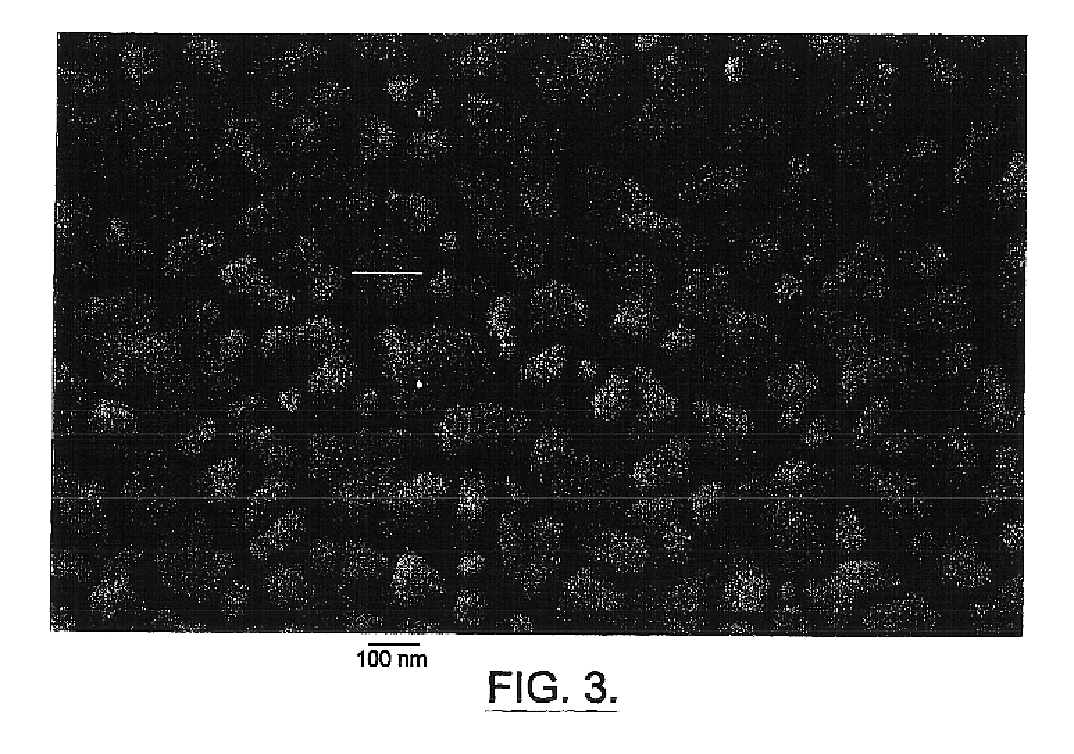
A two-mil, press-polished Fluorex® film, a polyvinylidene difluoride-acrylic film available from Rexam, was mounted upon a main roller (40° F.) in a closed system having a pressure of about 0.0001 Torr. The Fluorex® film was then plasma treated via 500 W of AC power with 125 standard cubic centimeters per minute (SCCM) of oxygen. Thereafter, a first discontinuous layer of indium islands was deposited via electron beam evaporation (0.11 amps; 6 kV) onto the Fluorexe film. The first discontinuous indium layer possessed an optical density (OD) of 1.15.
example 2
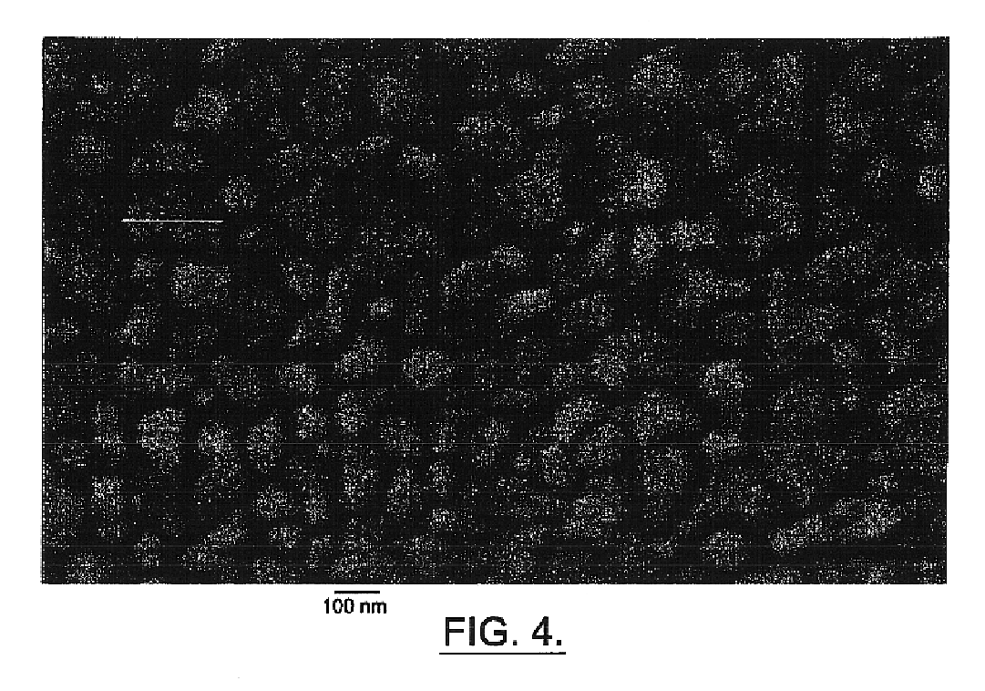
The first discontinuous indium layer of Example 1 was then plasma treated via 500 W of AC power with 125 SCCM of oxygen. After this plasma treatment, the first discontinuous indium layer exhibited significant oxidation. Then, a second discontinuous layer of indium islands was deposited via electron beam evaporation (0.11 amps; 6 kV) onto the first discontinuous indium layer. The second discontinuous layer of indium islands possessed an optical density (OD) of 1.15.
example 3
A second discontinuous layer of indium islands was deposited via electron beam evaporation (0.11 amps; 6 kV) onto the first discontinuous indium layer of Example 1, but unlike Example 2, the first discontinuous indium layer had not been plasma treated. The indium metallized film possessed a slightly yellowish color, similar to that that occurs when the indium islands are relatively large.
PUM
| Property | Measurement | Unit |
|---|---|---|
| roughness | aaaaa | aaaaa |
| weight percent | aaaaa | aaaaa |
| weight percent | aaaaa | aaaaa |
Abstract
Description
Claims
Application Information
 - R&D
- Intellectual Property
- Life Sciences
- Materials
- Tech Scout
- Unparalleled Data Quality
- Higher Quality Content
- 60% Fewer Hallucinations
Browse by: Latest US Patents, China's latest patents, Technical Efficacy Thesaurus, Application Domain, Technology Topic, Popular Technical Reports.
© 2025 PatSnap. All rights reserved.Legal|Privacy policy|Modern Slavery Act Transparency Statement|Sitemap|About US| Contact US: help@patsnap.com


