Methods for forming thin layers of materials on micro-device workpieces

a technology of micro-device workpieces and thin films, applied in the direction of coatings, chemical vapor deposition coatings, metallic material coating processes, etc., can solve the problems of high temperature, film quality and uniformity, reaction may occur in the gas phase prematurely before reaching the substrate, etc., and achieve the effect of reducing processing tim

Inactive Publication Date: 2005-03-01
MICRON TECH INC
View PDF99 Cites 43 Cited by
  • Summary
  • Abstract
  • Description
  • Claims
  • Application Information

AI Technical Summary

Benefits of technology

This embodiment accordingly provides a continuous pulse train in which discrete areas of the workpiece are exposed to one of the first or second precursors while adjacent areas are exposed to the purge gas. A continuous pulse train can accordingly be presented to the surface of the wafer without having to completely purge the first and second precursors from the entire surface area of the workpiece during each purge cycle. This is expected to greatly reduce the processing time for forming a layer of material on the workpiece.

Problems solved by technology

Such high temperatures are typically not desirable because heating the workpiece can be detrimental to the structures and other materials that are already formed on the workpiece.
On the other hand, if more reactive precursors are used so that the reaction temperature of the workpiece can be lower, then reactions may occur prematurely in the gas phase before reaching the substrate.
This is not desirable because the film quality and uniformity may suffer, and also because it limits the type of precursors that can be used.
Thus, CVD techniques may not be appropriate for many thin film applications.
One drawback of ALD processing is that the film thickness may be different at the center of the workpiece than at the periphery.
In practice, however, this may cause the film at the center of the workpiece to be thinner than the film at the periphery.
Moreover, the center portion of such plates may become coated with the solid material because it is difficult to purge all of the precursors from this portion of the gas distributor 60 during normal purge cycles.
Another drawback of ALD processing is that it has a low throughput compared to CVD techniques.
The low throughput of existing ALD techniques limits the utility of this technology in its current state because ALD may be a bottleneck in the fab.

Method used


Image

  • Methods for forming thin layers of materials on micro-device workpieces
  • Methods for forming thin layers of materials on micro-device workpieces
  • Methods for forming thin layers of materials on micro-device workpieces

Examples


Embodiment Construction

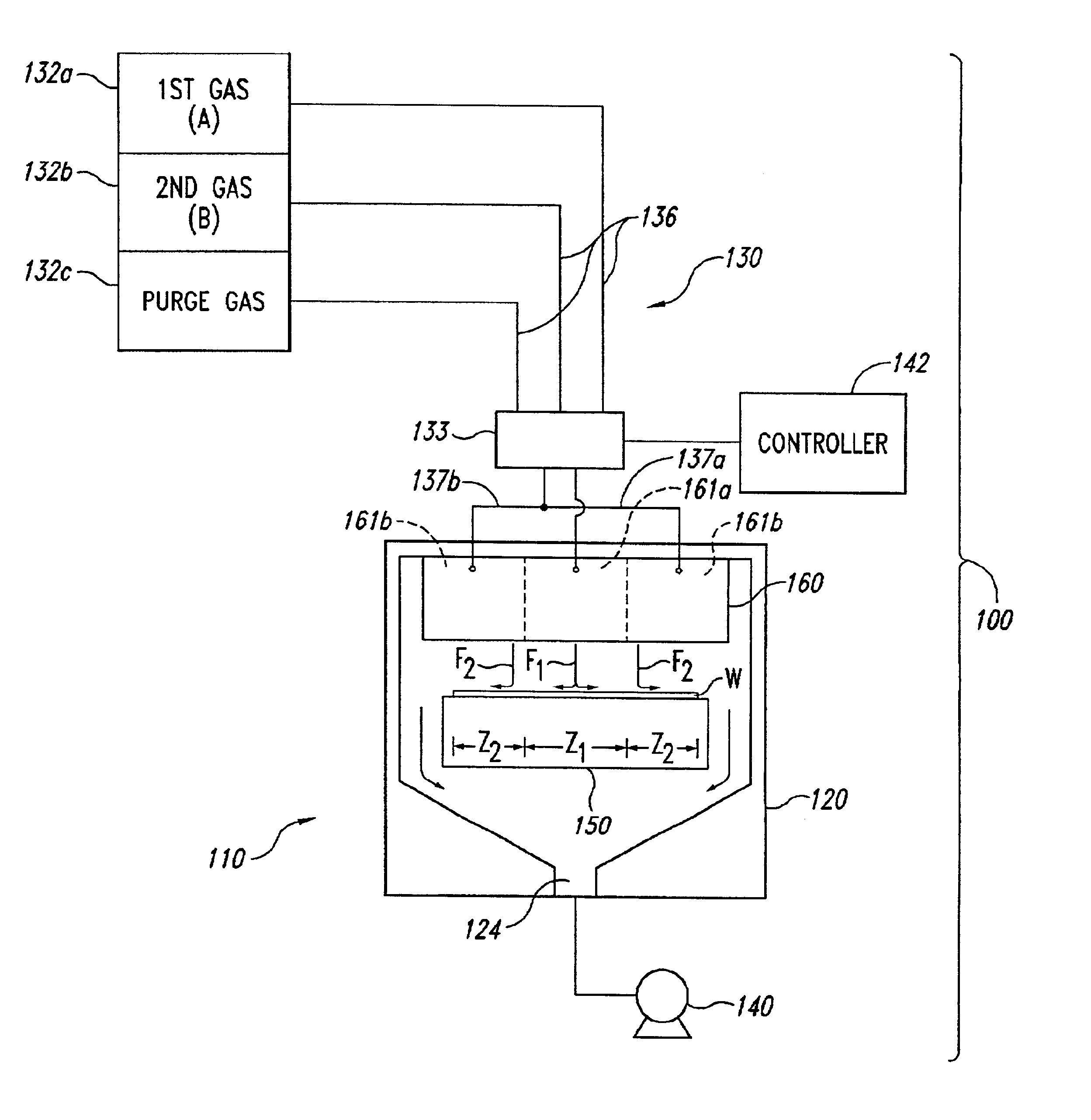
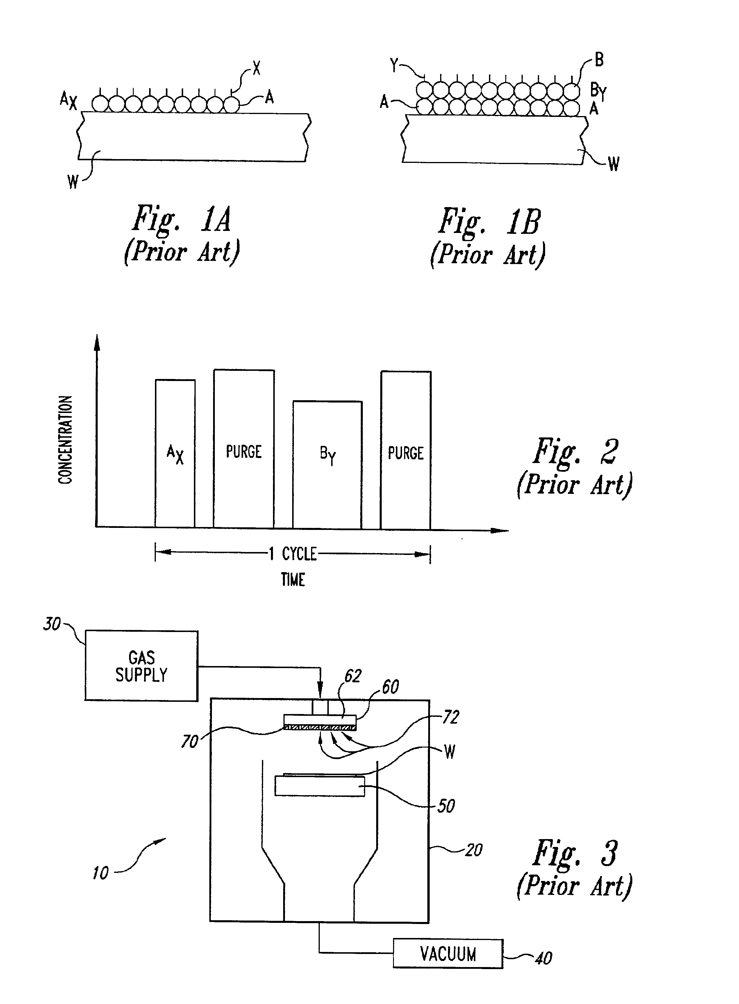
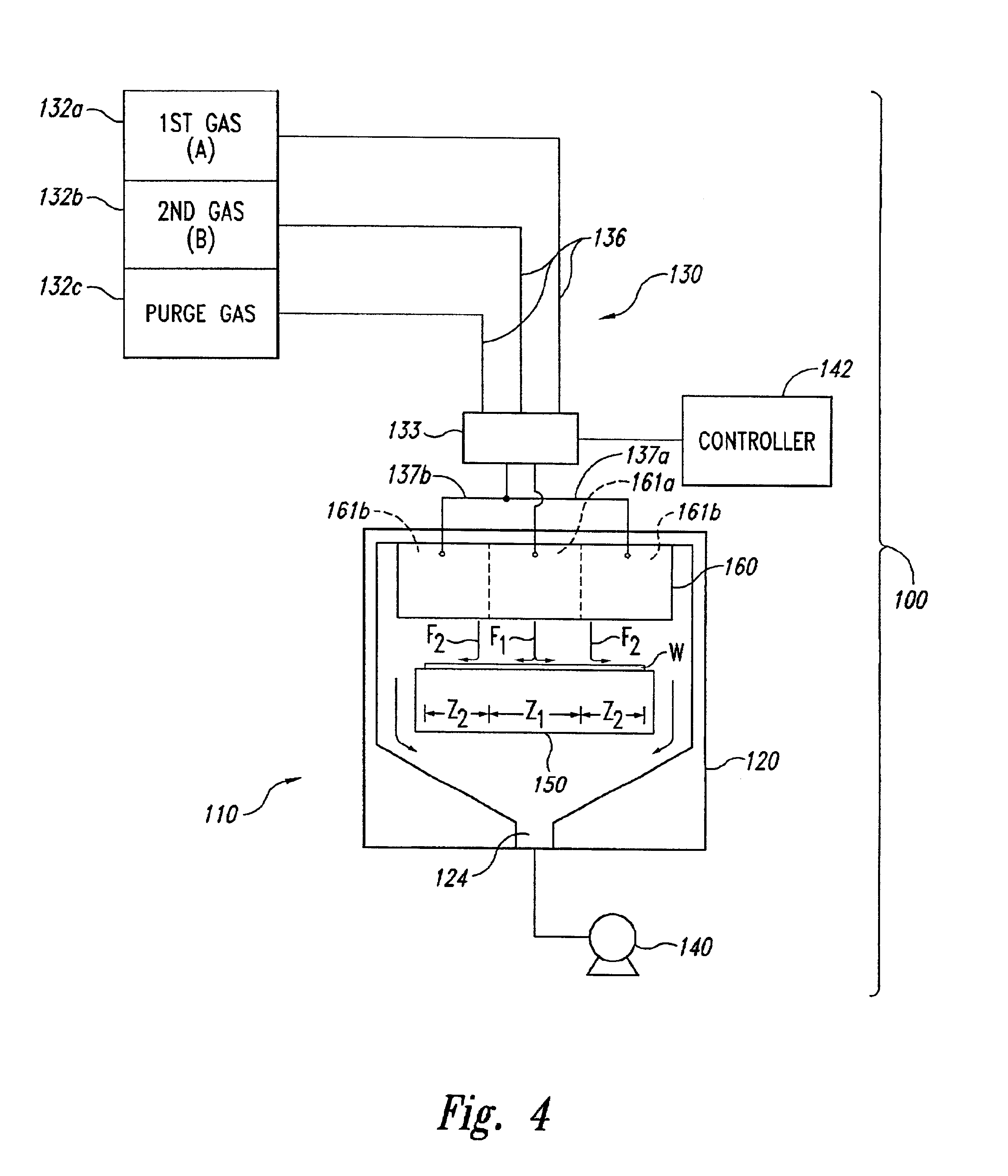
The following disclosure describes several embodiments of reactors for depositing a material onto a micro-device workpiece, systems including such reactors, and methods for depositing materials onto micro-device workpieces. Many specific details of the invention are described below with reference to depositing materials onto micro-device workpieces. The term “micro-device workpiece” is used throughout to include substrates upon which and / or in which microelectronic devices, micromechanical devices, data storage elements, read / write components, and other features are fabricated. For example, micro-device workpieces can be semiconductor wafers such as silicon or galium arsenide wafers, glass substrates, insulative substrates, and many other types of materials. The term “gas” is used throughout to include any form of matter that has no fixed shape and will conform in volume to the space available, which specifically includes vapors (i.e., a gas having a temperature less than the critic...


PUM

PropertyMeasurementUnit
thicknessaaaaaaaaaa
concentrationaaaaaaaaaa
sizeaaaaaaaaaa

Abstract

A method of forming a layer on a micro-device workpiece includes dispensing a first pulse of a first precursor at a first region of the workpiece to flow toward a second region of the workpiece. The second region of the workpiece is located radially outward relative to the first region of the workpiece. The embodiment of this method further includes dispensing a first pulse of a purge gas at the first region of the workpiece to flow toward the second region of the workpiece after terminating the first pulse of the first precursor. Additionally, this embodiment also includes dispensing a second pulse of a first precursor at the second region of the workpiece to flow radially outward concurrently with dispensing the first pulse of a purge gas in the first region of the workpiece. The first pulse of the purge gas is terminated at the first region of the workpiece, and the second pulse of the first precursor is terminated at the second region. At this stage, the method further includes dispensing a first pulse of a second precursor at the first region of the workpiece to flow radially outward toward the second region, and dispensing a second pulse of the purge gas at the second region of the workpiece to flow radially outward concurrently with the first pulse of the second precursor in the first region. A single cycle of the process can further include dispensing a third pulse of the purge gas onto the first region of the workpiece to flow radially outward after terminating the first pulse of the second precursor, and concurrently dispensing a second pulse of the second precursor in the second region to flow radially outward.

Description

TECHNICAL FIELDThe present invention is related to the field of thin film deposition in the manufacturing of microelectronic devices, micromechanical devices and other types of micro-devices.BACKGROUNDThin film deposition techniques are widely used in the manufacturing of microelectronic devices to form a coating on a workpiece that closely conforms to the surface typography. The size of the individual components in the devices is constantly decreasing, and the number of layers in the devices is increasing. As a result, the density of components and the aspect ratios of depressions (e.g., the ratio of the depth to the size of the opening) is constantly increasing. The size of the workpieces is also increasing to provide more real estate for forming more dies (i.e., chips) on a single workpiece. Many fabricators, for example, are transitioning from 200 mm to 300 mm workpieces, and even larger workpieces will likely be used in the future. Thin film deposition techniques accordingly st...

Claims


Application Information

Patent Timeline
Patent Type & Authority Patents(United States)
IPC IPC(8): C23C16/455C23C16/44
CPCC23C16/45527C23C16/45574C23C16/45565
Inventor DERDERIAN, GARO J.SANDHU, GURTEJ
Owner MICRON TECH INC
Why Eureka
Try Eureka