Method for backside alignment of photo-processes using standard front side alignment tools

a technology of front side alignment and backside processing, which is applied in the direction of photomechanical equipment, instruments, optics, etc., can solve the problems of high cost of alignment tools, high cost of backside processing of silicon wafers, and high cost of both solutions in application

Inactive Publication Date: 2005-03-01
IBM CORP
View PDF6 Cites 29 Cited by
  • Summary
  • Abstract
  • Description
  • Claims
  • Application Information

AI Technical Summary

Problems solved by technology

Backside processing of silicon wafers provides many challenges.
Currently, costly alignment tools are utilized to visually inspect the bottom of the wafer once the wafer is turned over (the former wafer top), for alignment marks while aligning subsequent masks to the wafer top (former wafer bottom).
Both solutions are costly and time consuming in application.

Method used


Image

  • Method for backside alignment of photo-processes using standard front side alignment tools
  • Method for backside alignment of photo-processes using standard front side alignment tools
  • Method for backside alignment of photo-processes using standard front side alignment tools

Examples


Embodiment Construction

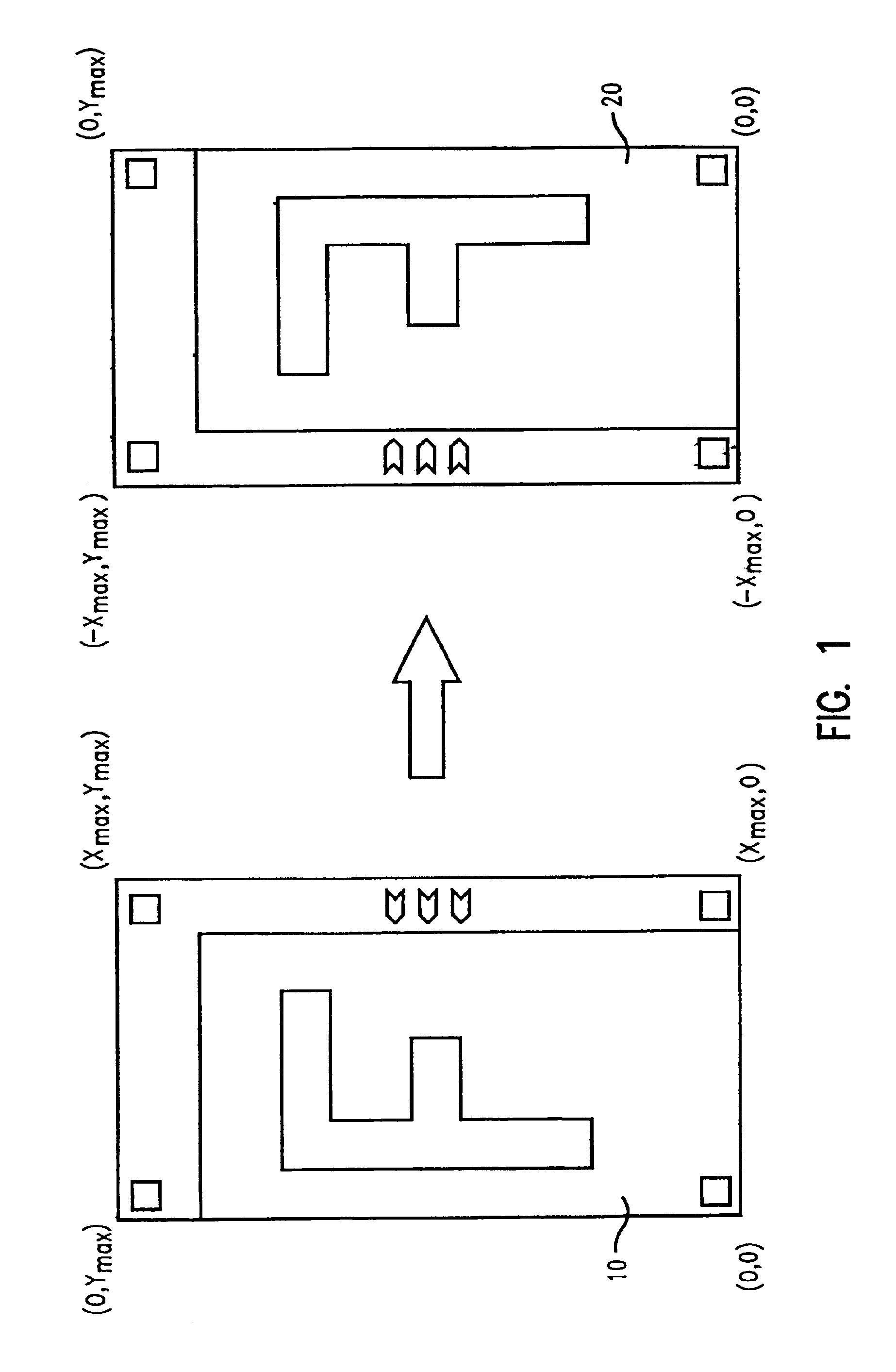
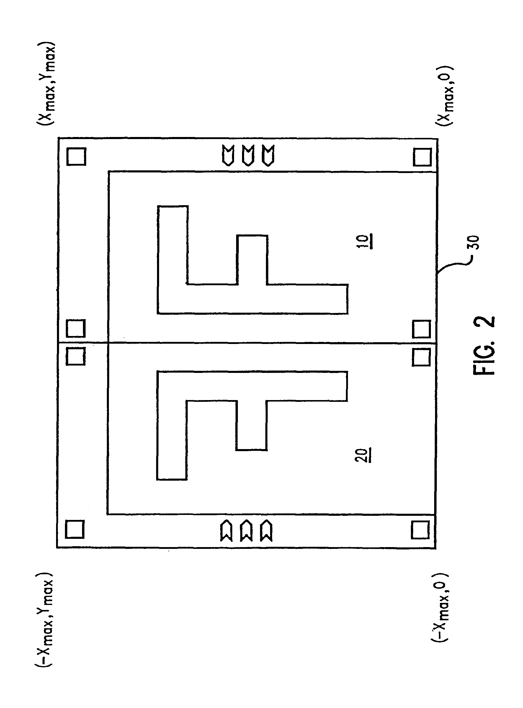
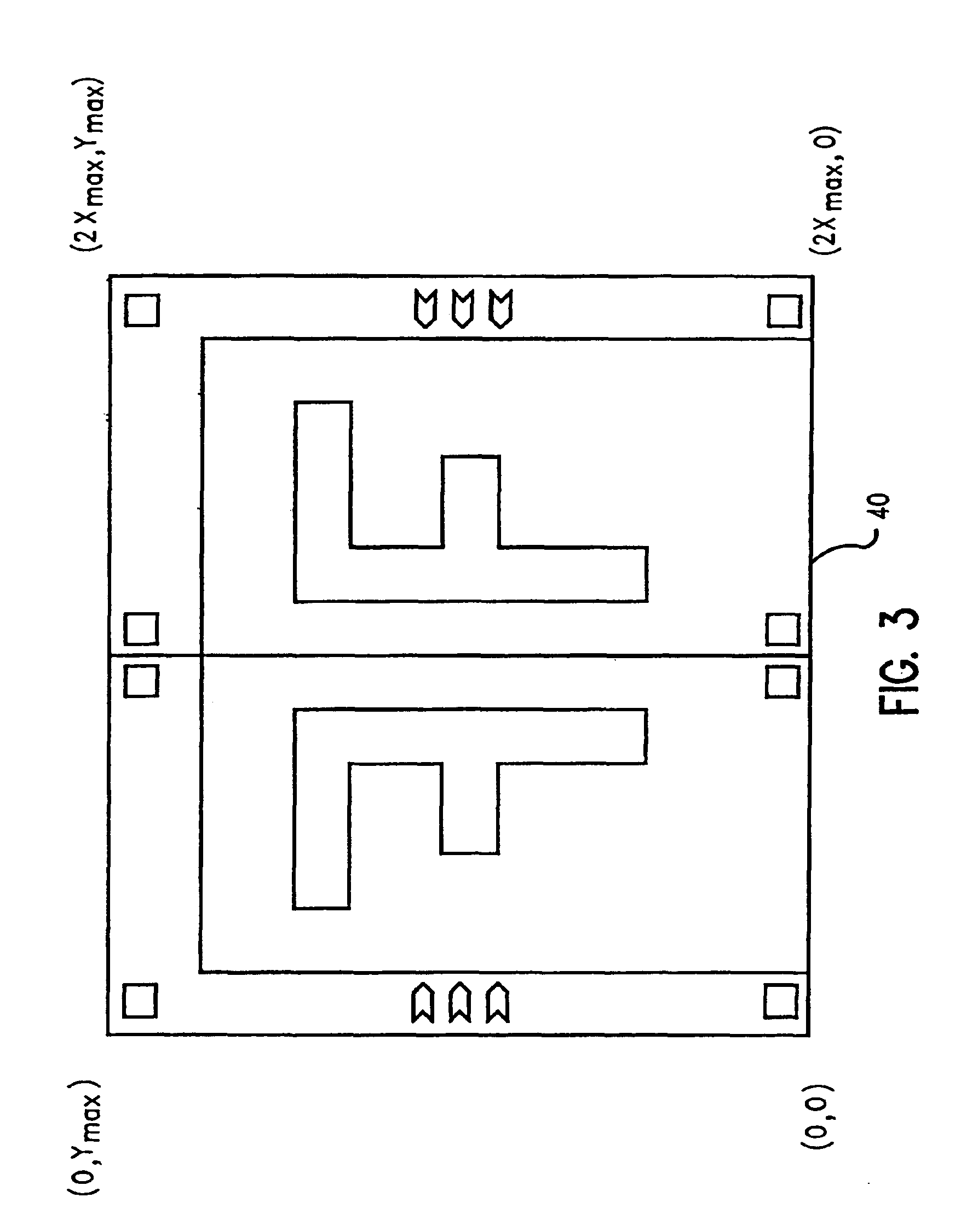
In describing the preferred embodiment of the present invention, reference will be made herein to FIGS. 1-5 of the drawings in which like numerals refer to like features of the invention.

The present invention provides a mirror image of the integrated circuit chip and scribe channel or kerf within a single optical field. When the wafer is flipped over or reversed, the chip appears the same as it is on the first side, that is, equal to its own mirror image. Prior to the backside lithography, wafer is flipped, bonded to a secondary substrate or given other means of mechanical support, and then a backside grind or etch is performed on the wafer such that the front side alignment marks are detected from the backside. These alignment marks are preferably on a trench mask or level, a device isolation level, or the like, but may be on other masks as well. Once the alignment marks are made detectable, the lithography may continue as though the wafer was not flipped over at all. Thus, no spec...


PUM

PropertyMeasurementUnit
optical fieldaaaaaaaaaa
dimensionaaaaaaaaaa
photosensitiveaaaaaaaaaa

Abstract

An image of an integrated circuit chip and optical kerf and their mirror image are formed within a single optical field. When a substrate pattern using this process is flipped over or reversed, the processed pattern appears the same as on the first side, equal to its own mirror image. Prior to the backside lithography, a portion of the second side is removed to allow detection of alignment marks on the first side from the second side of the substrate. Once the alignment marks are detected, the lithography continues as though the substrate was not flipped over at all.

Description

BACKGROUND OF INVENTIONThe present invention relates generally to aligning patterns on substrates, and in particular, to accurate front-to-back alignment of patterns on a semiconductor wafer.In semiconductor manufacturing, the processing steps for fabricating a semiconductor device involve exposing a substrate using a lithographic exposure system, such as exposing a semiconductor wafer coated with photosensitive material. This exposure requires aligning a reticle having a pattern of a particular device layer to an existing pattern on the substrate. After alignment, the reticle is exposed to radiation to which the photosensitive coating is sensitive, which transfers the reticle pattern onto the wafer.Alignment marks and the alignment of subsequent lithographic patterns with respect to those marks are an important part of the semiconductor manufacturing process. Alignment of one pattern layer to previous layers is typically done with the assistance of special alignment patterns design...

Claims


Application Information

Patent Timeline
Patent Type & Authority Patents(United States)
IPC IPC(8): G01B11/00G03F9/00G03F7/20
CPCG03F7/70425G03F9/7084G03F9/7003
Inventor PAGETTE, FRANCOISSCHNABEL, CHRISTOPHER M.
Owner IBM CORP
Why Eureka
Try Eureka