Three dimensional microstructures and method of making

a microstructure and three-dimensional technology, applied in the field of three-dimensional microstructures and making methods, can solve the problems of other very complex devices that are not integrated circuits, drawbacks inherent in building such structures out of silicon materials, and hinder the wide adaptation of devices fabricated with such materials

Inactive Publication Date: 2005-03-01
BATTELLE MEMORIAL INST
View PDF6 Cites 31 Cited by
  • Summary
  • Abstract
  • Description
  • Claims
  • Application Information

AI Technical Summary

Benefits of technology

It is a further object of the present invention to provide a microfabrication method for forming complex, three-dimensional structures that utilizes off the shelf photosensitive materials.
The second layer is then patterned in the same manner as the first, by applying an external stimulus to create voids in the second layer and removing any material present in those voids. In this manner, successive layers of the photosensitive material can be individually patterned and stacked upon one and another, thereby allowing the creation of highly complex, three dimensional microstructures having virtually unlimited geometries. Voids are preserved, either in whole or in part, in each successive layer by the presence of the sacrificial material. Thus, an additional step of removing the sacrificial material after the addition of the second layer, or after the addition of a series of successive layers, allows the patterns formed in the layers to form into a complex, three dimensional, structures on a micro scale.
While the simplest example of the present invention is a three dimensional structure built of only two layers of photosensitive materials, the technique of the present invention that allow the creation of a two layer structure can be repeated for an infinite number of successive layers, thereby allowing the creation of highly complex three dimensional structures made of many layers stacked on top of one and another. This is accomplished simply by adding additional successive layers of photosensitive material, applying an external stimulus to each successive layer of photosensitive material, thereby creating voids in each additional layer, removing any material present in the voids, providing additional successive layers of sacrificial material within at least a portion of the voids and interspaced between each of the additional successive layers of photosensitive material, and removing the layers of sacrificial materials.

Problems solved by technology

Despite the very small scale, the precision fabrication techniques that have enabled the fabrication of complex integrated circuits, such as modern microprocessors, have allowed other very intricate devices that are not integrated circuits to be designed and built using these techniques.
While complicated devices such as the micromachined mass spectrometer have been developed, there still exist drawbacks inherent in building such structures out of silicon materials.
One drawback that may have hindered the wide adaptation of devices fabricated with such materials is a failure on the part of designers to devise simple methods and techniques for readily using these materials in the fabrication of complex, three-dimensional structures, particularly methods and techniques that lend themselves to high levels of automation, and thus repeatable results.

Method used


Image

  • Three dimensional microstructures and method of making

Examples


Embodiment Construction

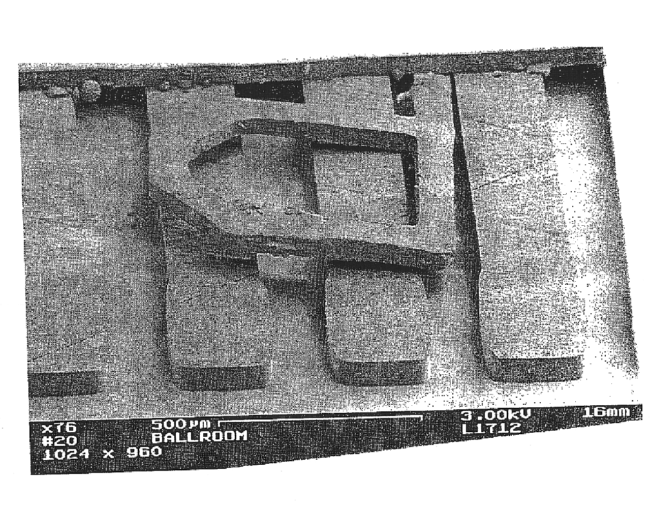
A series of experiments were conducted to demonstrate the principles of the present invention. These experiments demonstrated the fabrication of free-standing micro components and fabrication of closed tunnels or conduits of essentially unlimited length / cross-sectional area ratio. The structures resulting from these experiments are shown the two electron micrographs, FIG. 1. A letter “P” was fabricated on a release layer, then captured with micro tools and moved so that its foot penetrated a conduit. The conduit is 150 microns wide, 50 microns tall, and 10,000 microns long.

The photolithographic processing of these devices was carried out using a commercially available photosensitive material and solvent system, specifically SU8-50C from Microchem Corporation of Newton, Mass. The “50” denotes viscosity, which ranges from 5 to 500 in Microchem's arbitrary labeling. The “C” represents an alternative solvent chosen for lower toxicity but which is also less polar than the standard solven...


PUM

PropertyMeasurementUnit
aspect ratiosaaaaaaaaaa
thicknessaaaaaaaaaa
electrostatic potentialaaaaaaaaaa

Abstract

A method of forming complex three-dimensional microstructures wherein an external stimulus is applied to a first layer of a photosensitive material, thereby creating voids in the first layer, and any material present in those voids is removed. A sacrificial material is then provided within at least a portion of the voids. This sacrificial layer fills the voids, either in whole or in part, and enables a second layer of photosensitive material to be stacked upon the first, while still preserving the pattern formed in the first layer. Once the sacrificial layer has been applied, a second layer of photosensitive material may then be stacked onto the first. Successive layers of photosensitive material and sacrificial material may be added until a final, complex three-dimensional structure is created. The sacrificial material may then be removed with a solvent such as carbon dioxide.

Description

CROSS-REFERENCE TO RELATED APPLICATIONSNot ApplicableBACKGROUND OF THE INVENTIONThe techniques and materials used in the fabrication of integrated circuits and semiconductors have been applied to a variety of different problems where the very small scale inherent in the devices fabricated with these materials and techniques offer advantages to the end users. Despite the very small scale, the precision fabrication techniques that have enabled the fabrication of complex integrated circuits, such as modern microprocessors, have allowed other very intricate devices that are not integrated circuits to be designed and built using these techniques. One good example of the complexity possible in such devices is International Patent Application No. PCT / US94 / 10385, International Publication Number WO 95 / 12894 entitled “Micromachined Mass Spectrometer.” This disclosure describes a micromachined mass spectrometer fabricated on a silicon substrate.While complicated devices such as the micromachi...

Claims


Application Information

Patent Timeline
Patent Type & Authority Patents(United States)
IPC IPC(8): B81C1/00
CPCB81C99/0095B81C2201/0159B81C2201/0109B33Y10/00B33Y70/00
Inventor BOWMAN, LAWRENCE E.DUNHAM, GLEN C.
Owner BATTELLE MEMORIAL INST
Why Eureka
Try Eureka