Angular spectrum scanning quasi-confocal annular microstructure measuring device and method of array illumination

A measurement device and microstructure technology, applied in measurement devices, optical devices, microscopes, etc., can solve the problems of complex reflection, reduced measurement accuracy, enhanced background noise, etc., so as to improve detection signal strength, improve measurement accuracy, avoid The effect of complex reflections

Inactive Publication Date: 2013-11-27
HARBIN INST OF TECH
View PDF8 Cites 14 Cited by
  • Summary
  • Abstract
  • Description
  • Claims
  • Application Information

AI Technical Summary

Problems solved by technology

However, the above three methods converge parallel light beams to the surface of the sample for illumination through a microscope objective lens. When measuring a three-dimensional sample, due to the ups and downs of the surface profile of the sample itself, the converged illumina...

Method used


Image

  • Angular spectrum scanning quasi-confocal annular microstructure measuring device and method of array illumination
  • Angular spectrum scanning quasi-confocal annular microstructure measuring device and method of array illumination
  • Angular spectrum scanning quasi-confocal annular microstructure measuring device and method of array illumination

Examples


specific Embodiment 1

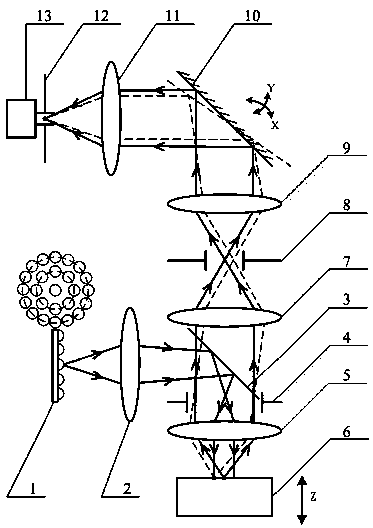
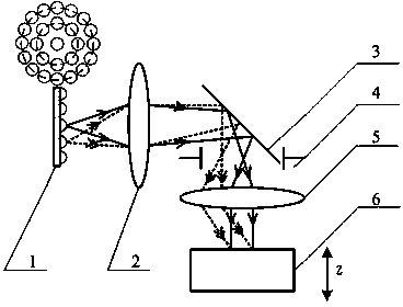
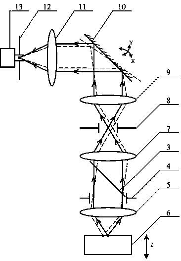
[0043] The structural schematic diagram of the angular spectrum scanning quasi-confocal annular microstructure measuring device of the array illumination of this embodiment is as follows: figure 1 As shown, the angular spectrum scanning illumination light path diagram is as figure 2 As shown, the quasi-confocal measurement optical path diagram is as image 3 Shown.

[0044] The measuring device includes an angular spectrum scanning illumination light path and a quasi-confocal measuring light path;

[0045] The angular spectrum scanning illumination light path includes: a concentric ring light source 1, an imaging lens 2, a dichroic prism 3, a first diaphragm 4 and a microscope objective lens 5; the light beams emitted from the concentric ring light source 1 sequentially pass through the imaging lens 2 After the spectroscopic prism 3 and the microscope objective lens 5, they are irradiated in parallel to the surface of the circularly symmetrical microstructure sample that moves alon...

specific Embodiment 2

[0064] The difference between this embodiment and the first embodiment is that the radius difference between two adjacent rings of the concentric ring light source 1 is not constant, and its beneficial effect is that it can be adjusted more accurately within a certain illumination angular spectrum range.

specific Embodiment 3

[0065] The difference between this embodiment and the first embodiment is that in the angular spectrum scanning quasi-confocal ring microstructure measurement method of the array illumination, the sequence of step d is preferably step d3, step d1, and step d2; The fastest step d2 is placed in the innermost layer, and the slowest step d3 is placed in the outermost layer. The beneficial effect is that it can reduce the time required for the angular spectrum illumination image and improve the three-dimensional shape of the circularly symmetrical microstructure sample. Appearance reconstruction efficiency.


PUM


Abstract

The invention discloses an angular spectrum scanning quasi-confocal annular microstructure measuring device and method of array illumination, and belongs to the field of ultra-precision three-dimensional microstructure surface morphology measurement. The device is designed to be provided with an angular spectrum scanning illumination light path; after sequentially passing through an imaging lens, a beam splitter prism and a microscope objective, beams emitted from a concentric annulus light source are shone onto the surface of a circularly-symmetrical microstructure sample to be measured in parallel, and different annular rings of the concentric annulus light source correspond to different angular spectra for illumination. According to the method, tomographic images of all the pixels under scanning illumination of different angular spectra are acquired first, then, on the basis of the confocal three-dimensional measurement principle, the axial coordinate of each pixel is judged, and finally the three-dimensional morphology of the microstructure sample to be measured is obtained in a fitting mode. Due to the design, an optimum illumination angle can be found for every part of the circularly-symmetrical microstructure sample to be measured, and the device and method avoid the problem that some areas can not be illuminated or complex reflection occurs to the areas, wherein the problem is caused by bumps of the surface profile of the circularly-symmetrical microstructure sample to be measured. Detection signal strength is promoted, background noise is lowered, and measurement precision is improved.

Description

Technical field [0001] An array-illuminated angular spectrum scanning quasi-confocal annular microstructure measuring device and method belong to the field of ultra-precision three-dimensional microstructure surface topography measurement. Background technique [0002] The processing applications of microstructures are mainly embodied in three aspects: microelectronics technology, microsystem technology and micro-optical technology, such as computer chips, biochips, and microlens arrays. The common feature of the above-mentioned technologies is that they have a three-dimensional structure and the size of the functional structure is on the order of micrometer, submicrometer or nanometer. The micro-nanoization of this structure not only brings about the saving of energy and raw materials, but also promotes the progress of modern technology and directly drives The development of related industries. With the rapid development of micro-processing technology, instruments that can per...

Claims


Application Information

Patent Timeline
IPC IPC(8): G01B11/24G02B21/00G02B21/06
Inventor 刘俭谭久彬王宇航
Owner HARBIN INST OF TECH
Why Eureka
Try Eureka