Vertical-structure LED chip and manufacturing method thereof

A LED chip and vertical structure technology, applied in the direction of electrical components, circuits, semiconductor devices, etc., can solve the problems of poor side wall coverage, etc., to achieve the effect of improving quality, good light angle, and increased light output rate

Inactive Publication Date: 2015-07-08
ENRAYTEK OPTOELECTRONICS
View PDF4 Cites 6 Cited by
  • Summary
  • Abstract
  • Description
  • Claims
  • Application Information

AI Technical Summary

Problems solved by technology

However, the sidewall coverage of the SiO2 passivation layer deposited by PECVD is poor, so the protective layer on the roughened surface of the vertical structure needs to be optimized.

Method used


Image

  • Vertical-structure LED chip and manufacturing method thereof
  • Vertical-structure LED chip and manufacturing method thereof
  • Vertical-structure LED chip and manufacturing method thereof

Examples


Embodiment Construction

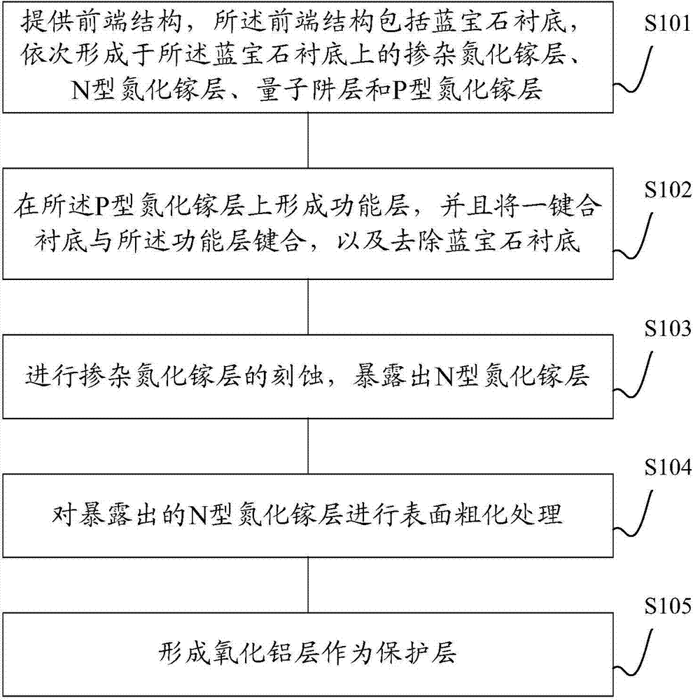
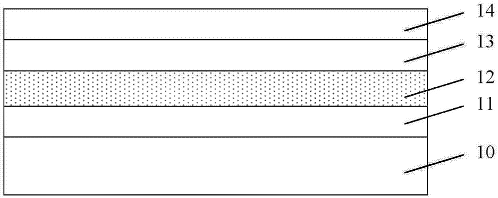
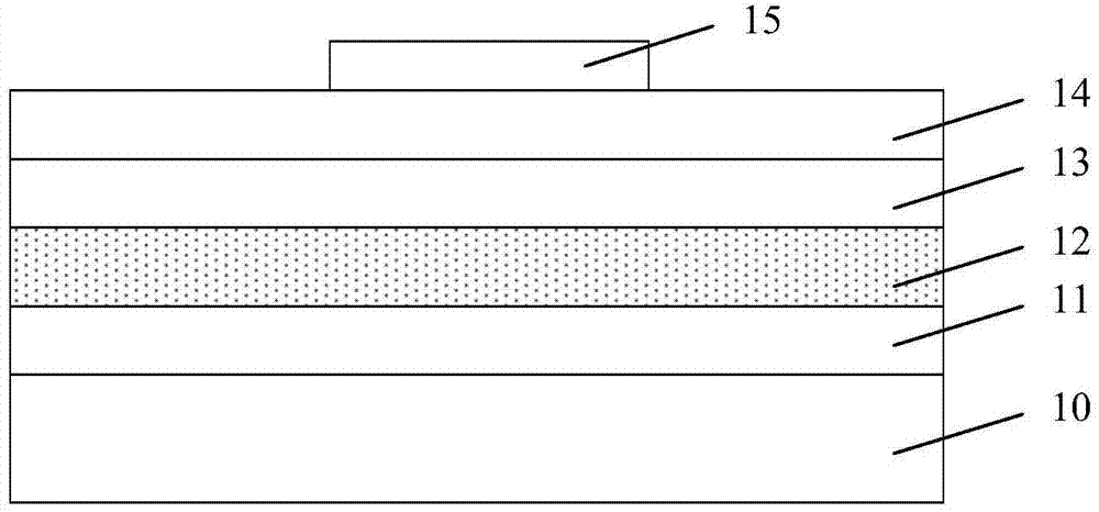
[0029] The vertical structure LED chip of the present invention and its manufacturing method will be described in more detail below in conjunction with schematic diagrams, wherein a preferred embodiment of the present invention is represented, it should be understood that those skilled in the art can modify the present invention described here, and still realize the present invention Beneficial effects of the invention. Therefore, the following description should be understood as the broad knowledge of those skilled in the art, but not as a limitation of the present invention.

[0030] In the following paragraphs the invention is described more specifically by way of example with reference to the accompanying drawings. Advantages and features of the present invention will be apparent from the following description and claims. It should be noted that all the drawings are in a very simplified form and use imprecise scales, and are only used to facilitate and clearly assist the ...


PUM

PropertyMeasurementUnit
transmittivityaaaaaaaaaa

Abstract

The invention discloses a manufacturing method of a vertical-structure LED chip. The manufacturing method comprises the steps that a front end structure is provided, wherein the front end structure comprises a sapphire substrate, a doped gallium nitride layer, an N-type gallium nitride layer, a gallium nitride layer and a P-type gallium nitride layer, and the doped gallium nitride layer, the N-type gallium nitride layer, the gallium nitride layer and the P-type gallium nitride layer are sequentially formed on the sapphire substrate; a function layer is formed on the P-type gallium nitride layer, a bonding substrate is bonded with the function layer, and the sapphire substrate is removed; the doped gallium nitride layer is etched, and the N-type gallium nitride layer is exposed; surface roughening processing is carried out on the exposed N-type gallium nitride layer; an aluminum oxide layer is formed as a protective layer. The invention further discloses the vertical-structure LED chip obtained through the method. According to the vertical-structure LED chip and the manufacturing method thereof, the light emitting rate can be improved, the better light emitting angle is obtained, and the light emitting efficiency and reliability of the vertical-structure LED chip are improved.

Description

technical field [0001] The invention relates to the technical field of semiconductors, in particular to a vertical structure LED chip and a manufacturing method thereof. Background technique [0002] For traditional front-mounted LED chips, P-type GaN is difficult to dope, resulting in low hole carrier concentration and difficulty in growing thick, resulting in difficult diffusion of current. At present, the method of preparing ultra-thin metal film or ITO film on the surface of P-type GaN is generally used to achieve The current has to spread evenly. However, the metal thin film electrode layer has to absorb part of the light to reduce the light extraction efficiency, and if the thickness is reduced, it will in turn limit the current diffusion layer to achieve uniform and reliable current diffusion on the surface of the P-type GaN layer. Although the light transmittance of ITO is as high as 90%, the electrical conductivity is not as good as that of metal, and the diffusion...

Claims


Application Information

Patent Timeline
Patent Type & Authority Applications(China)
IPC IPC(8): H01L33/44H01L33/00
CPCH01L33/44H01L33/0075H01L2933/0025
Inventor 张宇李起鸣徐慧文
Owner ENRAYTEK OPTOELECTRONICS
Why Eureka
Try Eureka